Semiconductor element and manufacturing method thereof
A manufacturing method and semiconductor technology, applied in semiconductor/solid-state device manufacturing, semiconductor devices, semiconductor/solid-state device components, etc., can solve problems such as potholes, uneven dielectric layer heights, and line bending, and achieve improved floating Coupling between gates and effect of narrowing trench aspect ratio
- Summary
- Abstract
- Description
- Claims
- Application Information
AI Technical Summary
Benefits of technology
Problems solved by technology
Method used
Image

Examples
Embodiment Construction
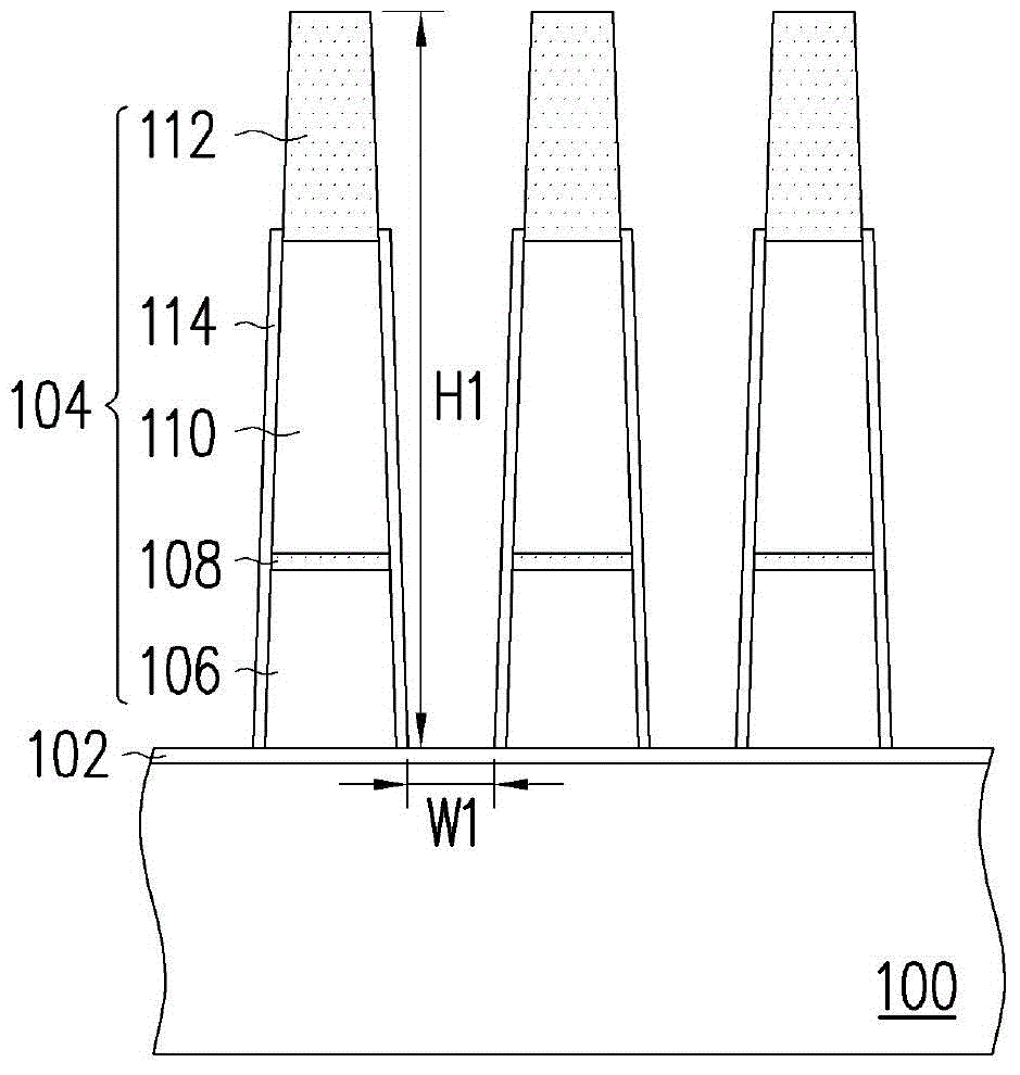
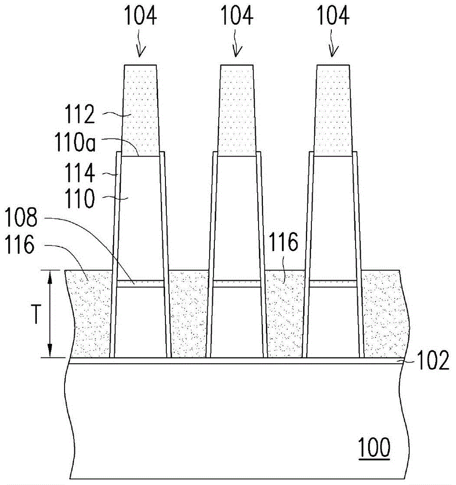
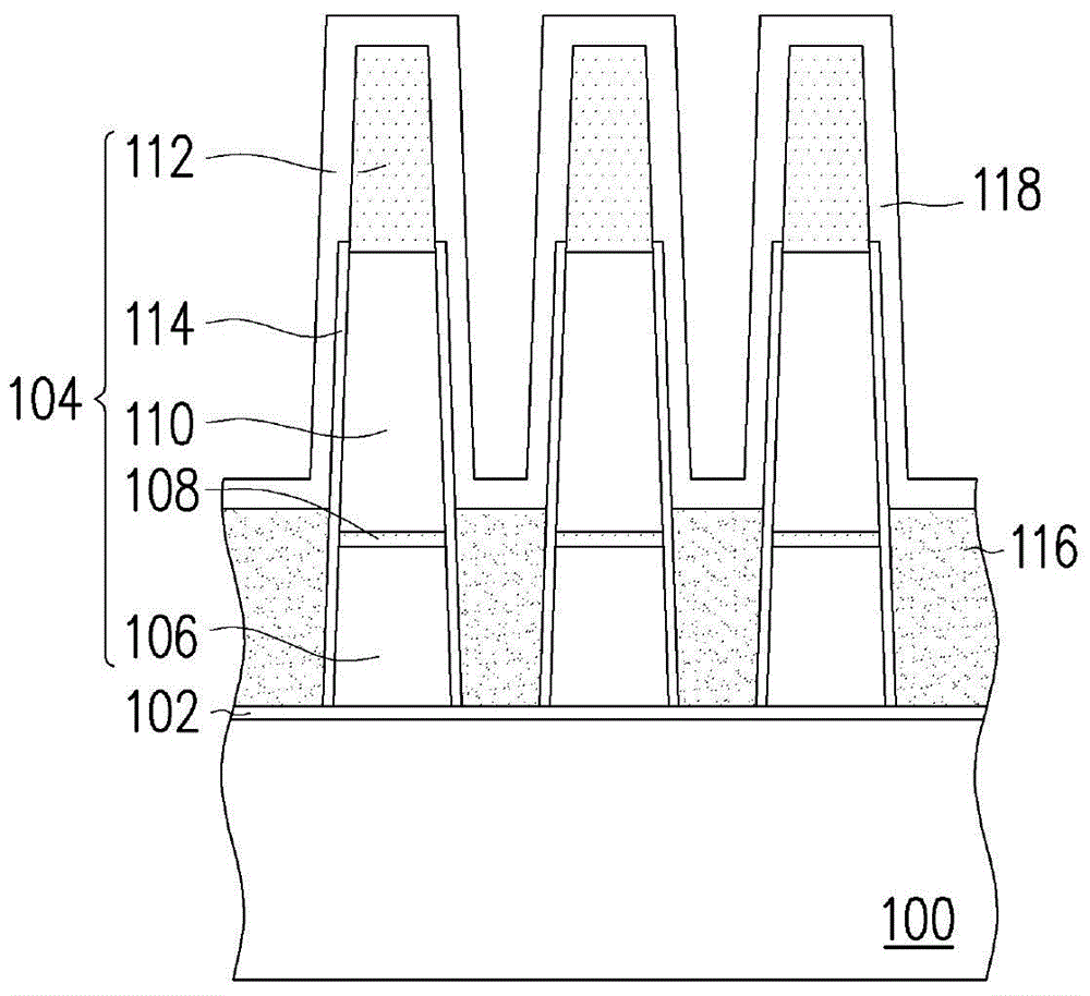
[0043] Figure 1A to Figure 1F It is a schematic cross-sectional view of a manufacturing process of a semiconductor device according to an embodiment of the present invention.
[0044] Please refer to Figure 1A Firstly, there is usually a thin film such as a gate insulating layer 102 on the surface of the substrate 100, and then stacked structures 104 have been formed on the substrate 100, wherein the aspect ratio of the grooves between the stacked structures 104 (height H1 to width W1 ratio) greater than 11, for example. When the aspect ratio of the grooves between the stacked structures 104 is greater than 11, it will be difficult to face the problem of difficult gap filling with the current technology of the present invention, and if the stacked structures 104 are conductor lines, they may also be bent under force in subsequent manufacturing processes. fold.
[0045] In this embodiment, each stack structure 104 includes, for example, a floating gate 106, an inter-gate diele
PUM
 Abstract
Description
Claims
Application Information
 - R&D Engineer
- R&D Manager
- IP Professional
- Industry Leading Data Capabilities
- Powerful AI technology
- Patent DNA Extraction
Browse by: Latest US Patents, China's latest patents, Technical Efficacy Thesaurus, Application Domain, Technology Topic.
© 2024 PatSnap. All rights reserved.Legal|Privacy policy|Modern Slavery Act Transparency Statement|Sitemap