Method for unloading wafer already subjected to surface process from silicon chip

A technology of wafers and silicon wafers, which is applied in the direction of electrical components, semiconductor/solid-state device manufacturing, circuits, etc., and can solve problems such as destroying the front pattern of the wafer, affecting the morphology of the electrode on the surface of the wafer and forward voltage parameters, etc.

Active Publication Date: 2017-01-11
WUXI CHINA RESOURCES HUAJING MICROELECTRONICS
View PDF4 Cites 0 Cited by
  • Summary
  • Abstract
  • Description
  • Claims
  • Application Information

AI Technical Summary

Benefits of technology

This technology allows wafers that have been processed beforehand to be loaded onto another substrate while maintain their electrical properties during processing. Unlike previous methods where they were treated differently after manufacturing, this new approach eliminates any negative impacts caused by these treatments.

Problems solved by technology

This patented technical problem addressed in this patents relates to efficiently handling and removing unwanted materials from wafer during manufacturing processes like chemical vapor deposition (CVD). Current solutions involve either high-thermal or corrosive techniques but these have limitations due to their ability to damage certain areas near the waference area where they were previously formed.

Method used


Image

  • Method for unloading wafer already subjected to surface process from silicon chip
  • Method for unloading wafer already subjected to surface process from silicon chip
  • Method for unloading wafer already subjected to surface process from silicon chip

Examples


Embodiment 1

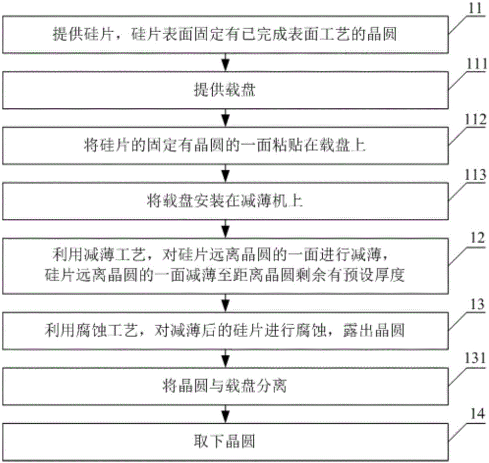
[0043] figure 1 It is a flow chart of a method for unloading a wafer that has completed a surface process from a silicon wafer provided by Embodiment 1 of the present invention. Such as figure 1 As shown, the method includes the following steps:

[0044] S11. Providing a silicon wafer, the surface of which is fixed with a wafer whose surface process has been completed.

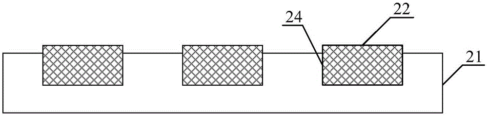
[0045] Such as figure 2 As mentioned above, the silicon wafer 21 in this embodiment is provided with at least one (only three are shown in the figure) wafer positioning grooves 24 , and the wafer 22 is fixed in the wafer positioning grooves 24 .

[0046] S12. Thinning the side of the silicon wafer away from the wafer by using a thinning process, the side of the silicon wafer away from the wafer is thinned to a predetermined thickness remaining from the wafer.

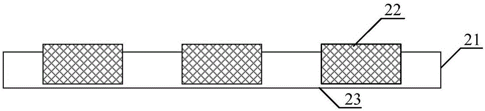
[0047] Such as image 3 As shown, there is remaining silicon 23 on the side away from the wafer 22 on the thinned silicon wafer 21 . The remaining

Embodiment 2

[0066] Figure 9 It is a flowchart of a method for unloading a wafer that has completed a surface process from a silicon wafer provided by Embodiment 2 of the present invention. Such as Figure 9 As shown, compared with the method of unloading the wafer with the completed surface process from the silicon wafer provided by the first embodiment of the present invention, this method only uses the thinning process to fix the wafer with the completed surface process. The silicon on the side of the silicon wafer away from the wafer is thinned until the wafer is exposed. At this time, since the silicon wafer has been thinned to expose the wafer, all the silicon on the side of the silicon wafer away from the wafer has been removed. Therefore, no further etching process is required to remove the remaining silicon on the side of the silicon wafer away from the wafer. Since no etching process is required, the impact of corrosion on the wafer can be completely avoided.

[0067] Compared w


PUM


Abstract

The invention discloses a method for unloading a wafer already subjected to a surface process from a silicon chip. The method comprises the steps of providing the silicon chip, wherein the wafer already subjected to the surface process is fixedly arranged on a surface of the silicon chip; thinning a surface, far away from the wafer, of the silicon chip by a thinning process; taking out the wafer when the surface, far away from the wafer, of the silicon chip is thinned until the wafer is exposed; corroding the thinned silicon chip by a corrosion process when the surface, far away from the wafer, of the silicon chip is thinned until the distance away from the wafer remains a preset thickness; and exposing the wafer, and taking out the wafer. With the method for unloading the wafer already subjected to the surface process from the silicon chip, provided by the embodiment of the invention, the wafer can be unloaded on the premise of no influence on wafer surface electrode morphology and a forward voltage parameter and no damage to a chip pattern on a front surface of the wafer.

Description


Claims


Application Information

Patent Timeline
Owner WUXI CHINA RESOURCES HUAJING MICROELECTRONICS
Why Eureka
Try Eureka