LED chip and manufacturing method therefor
A technology of LED chip and manufacturing method, which is applied in the direction of electrical components, circuits, semiconductor devices, etc., can solve the problems affecting the brightness and luminous efficiency of LED chips, and achieve the effects of improving light output efficiency, simple manufacturing method, and increasing luminous brightness
- Summary
- Abstract
- Description
- Claims
- Application Information
AI Technical Summary
Benefits of technology
Problems solved by technology
Method used
Image

Examples
Embodiment 1
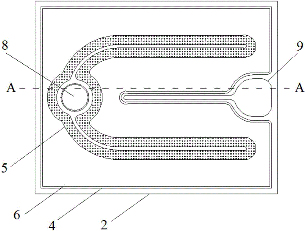
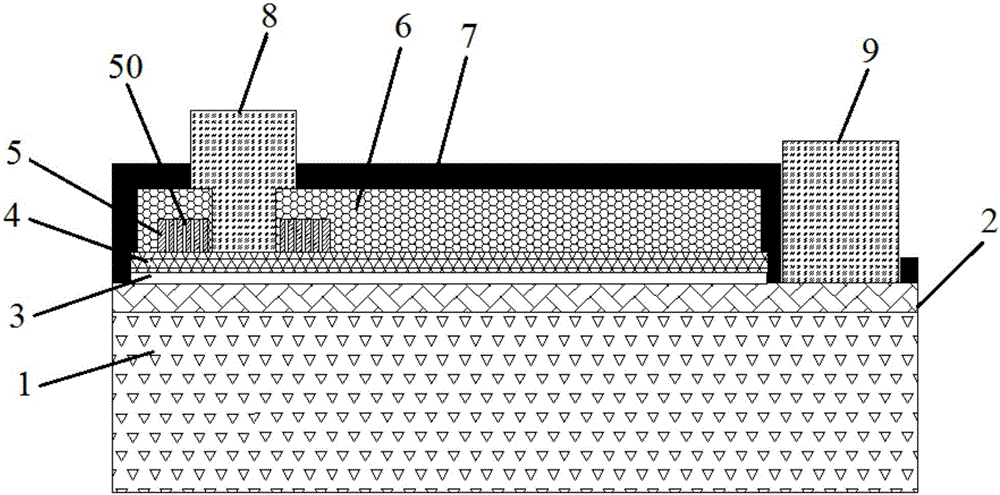
[0032] An embodiment of the present invention provides an LED chip, see figure 1 with figure 2 , the LED includes a substrate 1, and an n-type nitride semiconductor layer 2, a light-emitting layer 3, a p-type nitride semiconductor layer 4, a current blocking layer 5, a transparent conductive layer 6, and a p-type nitrogen semiconductor layer stacked on the substrate 1 in sequence. The compound semiconductor layer 4 is provided with a groove extending to the n-type nitride semiconductor layer 2, and the n-type nitride semiconductor layer 2, the sidewall of the groove, and the transparent conductive layer 6 are provided with a passivation layer 7, and the transparent conductive layer 6 The passivation layer 7 on the top is provided with a first through hole extending to the p-type nitride semiconductor layer 4, the p-type electrode 8 is arranged in the first through hole, and the passivation layer 7 on the n-type nitride semiconductor layer 2 There is a second through hole extend
Embodiment 2
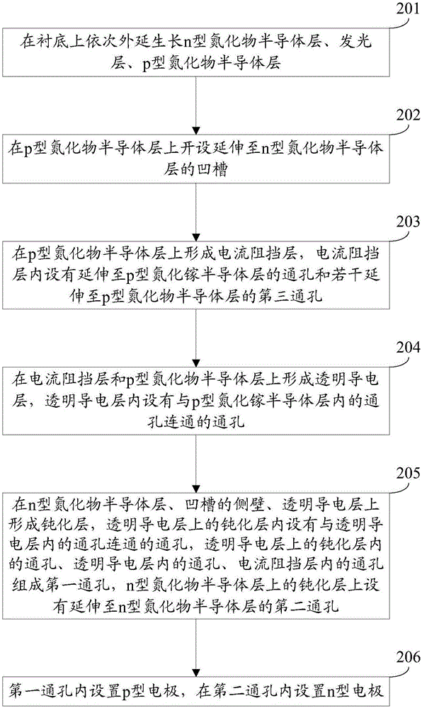
[0041] The embodiment of the present invention provides a method for manufacturing an LED chip, see image 3 , the production method includes:
[0042] Step 201: Epitaxially grow an n-type nitride semiconductor layer, a light-emitting layer, and a p-type nitride semiconductor layer on a substrate in sequence.
[0043] Specifically, the substrate can be a sapphire substrate, or a nitride semiconductor, such as SiN, GaN; the n-type nitride semiconductor layer can be an n-type doped GaN layer; the light-emitting layer can include alternately stacked InGaN quantum well layers and The GaN quantum barrier layer; the p-type nitride semiconductor layer may be a p-type doped GaN layer.
[0044] Step 202: Opening a groove extending to the n-type nitride semiconductor layer on the p-type nitride semiconductor layer.
[0045] Step 203 : forming a current blocking layer on the p-type nitride semiconductor layer, in which there are via holes extending to the p-type gallium nitride semiconduc
Embodiment 3
[0058] The embodiment of the present invention provides a method for manufacturing an LED chip, which is a specific implementation of the method provided in Embodiment 2. The method includes:
[0059] Step 301: Epitaxially grow an n-type nitride semiconductor layer, a light-emitting layer, and a p-type nitride semiconductor layer on the substrate by metal-organic chemical vapor deposition to form an epitaxial wafer.
[0060] Step 302: cleaning the epitaxial wafer, and opening a groove extending to the n-type nitride semiconductor layer on the p-type nitride semiconductor layer by using photolithography technology and dry etching technology.
[0061] Step 303: Deposit a silicon dioxide film on the epitaxial wafer by chemical vapor deposition technology, and wet-etch under the protection of the positive photoresist to form a current blocking layer covered with the third through hole, and remove the positive photoresist, the first step The cross-section of the three-way hole is a ci
PUM
 Abstract
Description
Claims
Application Information
 - R&D Engineer
- R&D Manager
- IP Professional
- Industry Leading Data Capabilities
- Powerful AI technology
- Patent DNA Extraction
Browse by: Latest US Patents, China's latest patents, Technical Efficacy Thesaurus, Application Domain, Technology Topic.
© 2024 PatSnap. All rights reserved.Legal|Privacy policy|Modern Slavery Act Transparency Statement|Sitemap