Organic light-emitting device and preparation method thereof
An electroluminescent device and electroluminescent technology, which are applied in the fields of electro-solid devices, semiconductor/solid-state device manufacturing, electrical components, etc., can solve the problems of low exciton recombination probability, low luminous efficiency of devices, etc., and are conducive to the transmission of electrons. , the chain segments are arranged in an orderly manner, and the effect of improving the luminous efficiency
- Summary
- Abstract
- Description
- Claims
- Application Information
AI Technical Summary
Problems solved by technology
Method used
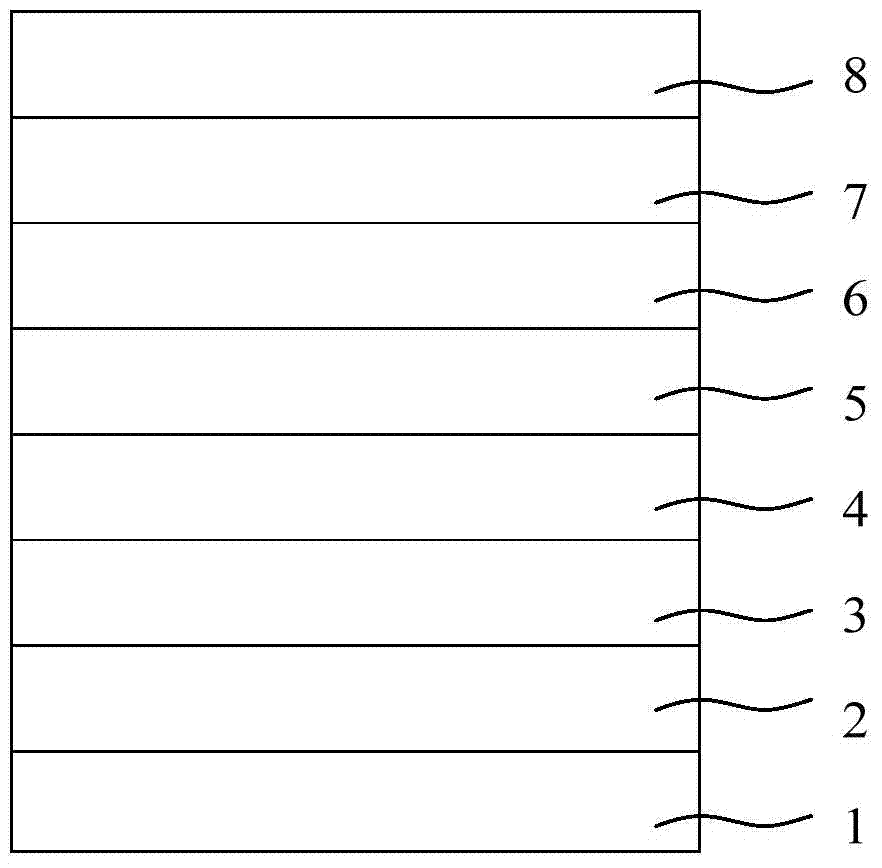
Image

Examples
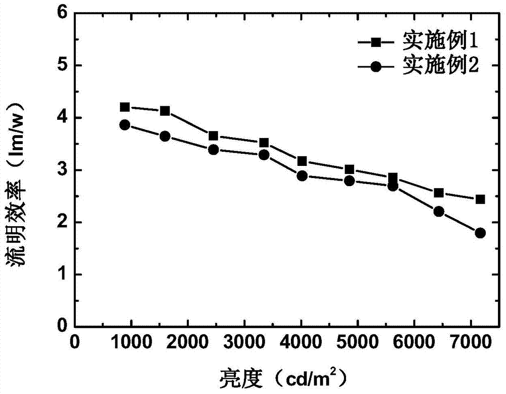
Embodiment 1
[0041] A method for preparing an organic electroluminescent device, comprising the following steps:
[0042] (1) Sonicate commercially available ordinary glass with detergent, deionized water, acetone, ethanol, and isopropanol for 15 minutes each to remove organic pollutants on the glass surface, clean it and air dry it; then use it on the glass substrate ITO with a thickness of 120nm was prepared by magnetron sputtering. The acceleration voltage of magnetron sputtering was 700V, the magnetic field was 120G, and the power density was 25W / cm 2 ; Then adopt the method of thermal resistance evaporation on the anode to prepare hole injection layer, hole transport layer, light-emitting layer and electron transport layer successively; Wherein,
[0043] The hole injection layer is made of MoO 3 , the pressure used in evaporation is 8×10 -4 Pa, the evaporation rate is 2nm / s, and the evaporation thickness is 25nm;
[0044] The material of the hole transport layer is NPB, and the pr
Embodiment 2
[0052] A method for preparing an organic electroluminescent device, comprising the following steps:
[0053] (1) Firstly, use detergent, deionized water, acetone, ethanol, and isopropanol to sonicate commercially available ordinary glass for 15 minutes each to remove organic pollutants on the glass surface, clean it and air dry it; then use it on the glass substrate AZO with a thickness of 300nm was prepared by magnetron sputtering. The acceleration voltage of magnetron sputtering was 300V, the magnetic field was 50G, and the power density was 40W / cm 2 ; Then adopt the method of thermal resistance evaporation on the anode to prepare hole injection layer, hole transport layer, light-emitting layer and electron transport layer successively; Wherein,
[0054] The material of the hole injection layer is WO 3 , the pressure used in evaporation is 2×10 -3 Pa, the evaporation rate is 10nm / s, and the evaporation thickness is 20nm;
[0055] The material of the hole transport layer
Embodiment 3
[0063] A method for preparing an organic electroluminescent device, comprising the following steps:
[0064] (1) Firstly, use detergent, deionized water, acetone, ethanol, and isopropanol to sonicate commercially available ordinary glass for 15 minutes each to remove organic pollutants on the glass surface, clean it and air dry it; then use it on the glass substrate AZO with a thickness of 150nm was prepared by magnetron sputtering. The acceleration voltage of magnetron sputtering was 800V, the magnetic field was 200G, and the power density was 1W / cm 2 ; Then adopt the method of thermal resistance evaporation on the anode to prepare hole injection layer, hole transport layer, light-emitting layer and electron transport layer successively; Wherein,
[0065] The material of the hole injection layer is WO 3 , the pressure used in evaporation is 5×10 -5 Pa, the evaporation rate is 1nm / s, and the evaporation thickness is 55nm;
[0066] The material of the hole transport layer i
PUM
| Property | Measurement | Unit |
|---|---|---|
| Thickness | aaaaa | aaaaa |
| Magnetic field | aaaaa | aaaaa |
| Power density | aaaaa | aaaaa |
Abstract
Description
Claims
Application Information
 - R&D Engineer
- R&D Manager
- IP Professional
- Industry Leading Data Capabilities
- Powerful AI technology
- Patent DNA Extraction
Browse by: Latest US Patents, China's latest patents, Technical Efficacy Thesaurus, Application Domain, Technology Topic.
© 2024 PatSnap. All rights reserved.Legal|Privacy policy|Modern Slavery Act Transparency Statement|Sitemap