Rounded corner triangle graphical substrate

A patterned substrate and triangular technology, applied in the direction of electrical components, circuits, semiconductor devices, etc., can solve the problems of high-quality growth and epitaxy, small gaps, etc., to broaden the process window, improve light extraction efficiency, and large pattern gaps Effect

Inactive Publication Date: 2017-08-11
HAIDIKE NANTONG OPTOELECTRONICS TECH CO LTD
View PDF8 Cites 0 Cited by
  • Summary
  • Abstract
  • Description
  • Claims
  • Application Information

AI Technical Summary

Benefits of technology

This patented technology allows for better control over growth conditions during semiconductor manufacturing by creating patterns on regular triangular shapes that are symmetrically arranged around certain sides of the basic shape. These patterns help increase the size of the spaces between neighboring rectangles while still keeping them evenly distributed throughout the entire surface area. By increasing this spacing, defects such as cracks caused when growing layers may be reduced without compromising their effectiveness. Additionally, these techniques allow for improved performance and increased lifespan of electronic devices made from silicone wafers used for photonics applications.

Problems solved by technology

This patents describes different ways to make efficient galium nitrogen semiconductor devices like blue laser diode (Blue Lamp Dot®) displays better than current technologies such as liquid state lamps. However, these techniques require expensive equipment and complex manufacturing processes, leading to lower device yields compared to existing methods. There has developed an improved method called silane bonding technique, where both the Group III element and Group V elements within each chip are transferred onto another material without requiring costly steps during production process. By utilizing this new approach, higher device yield rates may result from increased intravalence effects caused by smaller dimensions of the materials used instead of larger ones.

Method used


Image

  • Rounded corner triangle graphical substrate
  • Rounded corner triangle graphical substrate
  • Rounded corner triangle graphical substrate

Examples


Embodiment

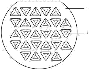
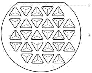
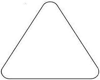
[0025] In this embodiment, the rounded triangle patterned substrate, such as figure 1 , 2 As shown in and 3, a sapphire substrate 1 is included, and the surface of the substrate 1 has periodic protrusions or depressions formed by a nanoimprint method. The length of the radian of the vertex angle is 0-500 nm.

[0026] In the embodiment, the rounded triangles are in a compact arrangement, that is, the perpendicular bisector of any side of each arranged rounded triangle passes through the center of the rounded triangle and the corresponding adjacent rounded triangle, and the adjacent rounded triangles are within the error range There is the same gap between them, the gap is 50-1000nm, and any side of the rounded triangle is arranged symmetrically with the side corresponding to the adjacent rounded triangle with respect to the gap axis; as an example, a more specific implementation is the period of the periodic pattern The length is 100-8000nm, the length of the bottom side of the


PUM

PropertyMeasurementUnit
Heightaaaaaaaaaa
Lengthaaaaaaaaaa

Abstract

The present invention relates to a rounded corner triangle graphical substrate. The rounded corner triangle graphical substrate comprises a substrate, periodization projections or depressed graphs are arranged around the surface of the substrate, the bottom edges of the projections or depressed graphs are rounded corner triangles and are closely arranged, namely the perpendicular bisector of any one edge of each arranged rounded corner triangle passes through the centers of the rounded corner triangle and the corresponding adjacent rounded corner triangle, there are gaps between adjacent rounded corner triangles, and any one edges of the arranged rounded corner triangles are axially symmetrical with the corresponding edges of the adjacent rounded corner triangle about the gap. The any one edge of the rounded corner triangle of the bottom edge is axially symmetrical with the corresponding edge of the adjacent rounded corner triangle, the rounded corner triangle graphical substrate has bigger figure gaps in the condition of keeping invariant duty ratio and compact arrangement so as to widen the epitaxial technical window and improve the product yield rate and reliability; and moreover, the rounded corner triangle is a traditional sharp-corner triangle to effectively prompt the dislocation bending and mutual annihilation in the epitaxial layers grown on the rounded corner triangle so as to improve the crystal quality of the epitaxial layers.

Description


Claims


Application Information

Patent Timeline
Owner HAIDIKE NANTONG OPTOELECTRONICS TECH CO LTD
Why Eureka
Try Eureka