Display device, array substrate and manufacturing method thereof

An array substrate and manufacturing method technology, applied in the display field, can solve the problems of shrinking, approaching the limit, and the inability to effectively realize the ultra-narrow frame of the panel, so as to achieve the effect of reducing the area and designing the ultra-narrow frame

Inactive Publication Date: 2017-10-03
WUHAN CHINA STAR OPTOELECTRONICS TECH CO LTD
View PDF5 Cites 5 Cited by
  • Summary
  • Abstract
  • Description
  • Claims
  • Application Information

AI Technical Summary

Problems solved by technology

[0002] With the continuous update of LCD panel technology, small-sized panels, especially 4-7 inch mobile phone panels, are gradually becoming thinner and lighter, with high screen-to-body ratio, ultra-narrow bezel and even bezel-less development. The traditional structure of LTPS (Low Temperature Poly-silicon (low temperature polysilicon) panel technology compresses the GOA circuit size, IC chip and reduces the distance between the lines, the frame is close to the level of 0.7mm and 0.8mm, but in order to ensure the effective operation of the GOA circuit and the reliability of the panel The test and various signal lines are separated from each other, and the compression of the frame, especially the lateral frame, is close to the limit
Unable to effectively realize the ultra-narrow frame of the panel design

Method used


Image

  • Display device, array substrate and manufacturing method thereof
  • Display device, array substrate and manufacturing method thereof
  • Display device, array substrate and manufacturing method thereof

Examples


Embodiment Construction

[0015] The present invention will be described in detail below by means of drawings and embodiments.

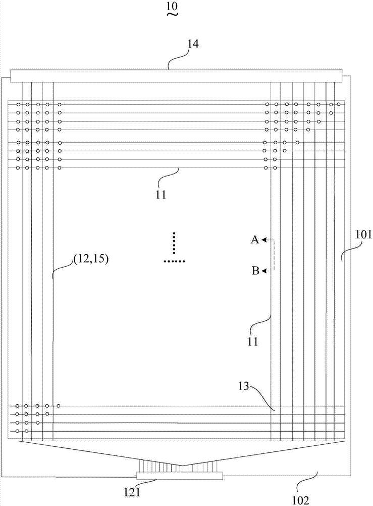
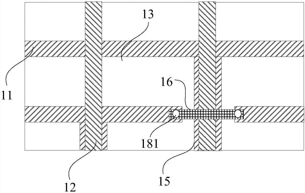
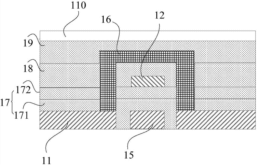
[0016] see figure 1 and image 3 , figure 1 is a schematic structural view of an array substrate provided by an embodiment of the present invention, figure 2 is a partial structure diagram of an array substrate provided by an embodiment of the present invention, image 3 is a schematic cross-sectional structure diagram of an array substrate provided by an embodiment of the present invention. The array substrate 10 includes a display area 101 and a non-display area 102 . The display area 101 is provided with multiple scan lines 11 , multiple data lines 12 intersecting the multiple scan lines 11 , and multiple pixel units 13 surrounded by the intersecting scan lines 11 and data lines 12 . The non-display area 102 is provided with a driving circuit 14 for providing a driving signal to the scan line 11 and a driving circuit 15 for providing a data voltage signal to the data...


PUM


Abstract

The invention discloses a display device, an array substrate and a manufacturing method thereof. The array substrate comprises a display area and a non-display area; a plurality of scanning lines, a plurality of data lines and a plurality of pixel units are arranged in the display area, the data lines are intersected with the scanning lines, and the pixel units are formed by enclosure of the intersected scanning lines and the data lines; a driving circuit for providing driving signals for the scanning lines is arranged in the non-display area and positioned in an extension direction of the data lines, so that the area of the non-display area in an extension direction of the scanning lines can be reduced. Consequently, a narrow bezel design of the display device can be realized.

Description

technical field [0001] The present invention relates to the field of display technology, in particular to a display device, an array substrate and a manufacturing method thereof. Background technique [0002] With the continuous update of LCD panel technology, small-sized panels, especially 4-7 inch mobile phone panels, are gradually becoming thinner and lighter, with high screen-to-body ratio, ultra-narrow bezel and even bezel-less development. The traditional structure of LTPS (Low Temperature Poly-silicon (low temperature polysilicon) panel technology compresses the GOA circuit size, IC chip and reduces the distance between the lines, the frame is close to the level of 0.7mm and 0.8mm, but in order to ensure the effective operation of the GOA circuit and the reliability of the panel The test and various signal lines are separated from each other, and the compression of the frame, especially the lateral frame, is close to the limit. The ultra-narrow frame of the panel des...

Claims


Application Information

Patent Timeline
IPC IPC(8): G02F1/1345
CPCG02F1/13454
Inventor 杨成奥
Owner WUHAN CHINA STAR OPTOELECTRONICS TECH CO LTD
Why Eureka
Try Eureka