Multiplication type organic photoelectric detector with narrowband and broadband optical detection capabilities
A technology of photodetector and detection capability, applied in the field of light detection, can solve problems such as difficulty in realizing narrow-band response, limiting practical application, etc., and achieve the effect of strong and weak light detection capability
- Summary
- Abstract
- Description
- Claims
- Application Information
AI Technical Summary
Benefits of technology
Problems solved by technology
Method used
Image

Examples
Embodiment 1
[0046] Embodiment 1 A multiplied organic photodetector with both narrowband and broadband light detection capabilities
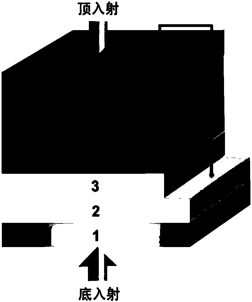
[0047] A multiplied organic photodetector with both narrowband and broadband light detection capabilities, including: a transparent substrate 1, a transparent anode 2, an anode modification layer 3, an active layer 4 and a semitransparent metal electrode 5, such as figure 1 shown.
[0048] The transparent substrate 1 is glass; the transparent electrode 2 is ITO; the transparent electrode modification layer 3 is PEDOT:PSS; the active layer 4 is a blend film of P3HT and PCBM with a mass ratio of 100:1 , with a thickness of 2.5 microns; the translucent metal cathode 5 is an aluminum electrode with a thickness of 16 nanometers.
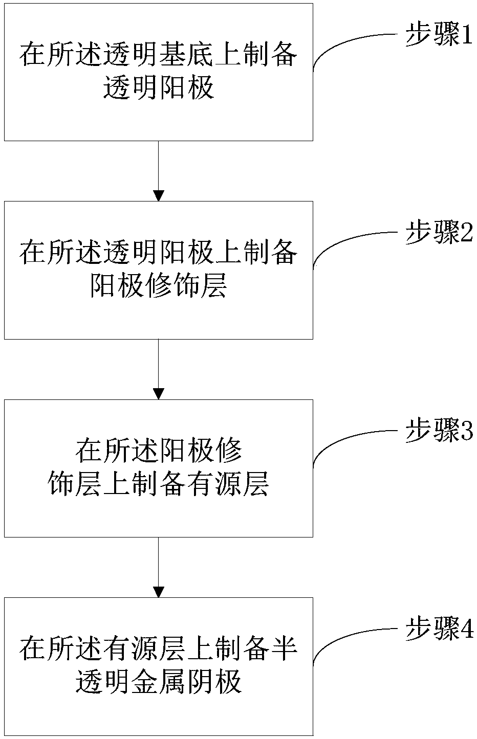
[0049] Such as figure 2 Shown, above-mentioned organic photodetector preparation method comprises the following steps:
[0050] Step 1: Prepare a transparent anode ITO on a glass substrate, then soak it in deionized water and absolute
Embodiment 2
[0057] Embodiment 2 A multiplied organic photodetector with both narrowband and broadband light detection capabilities
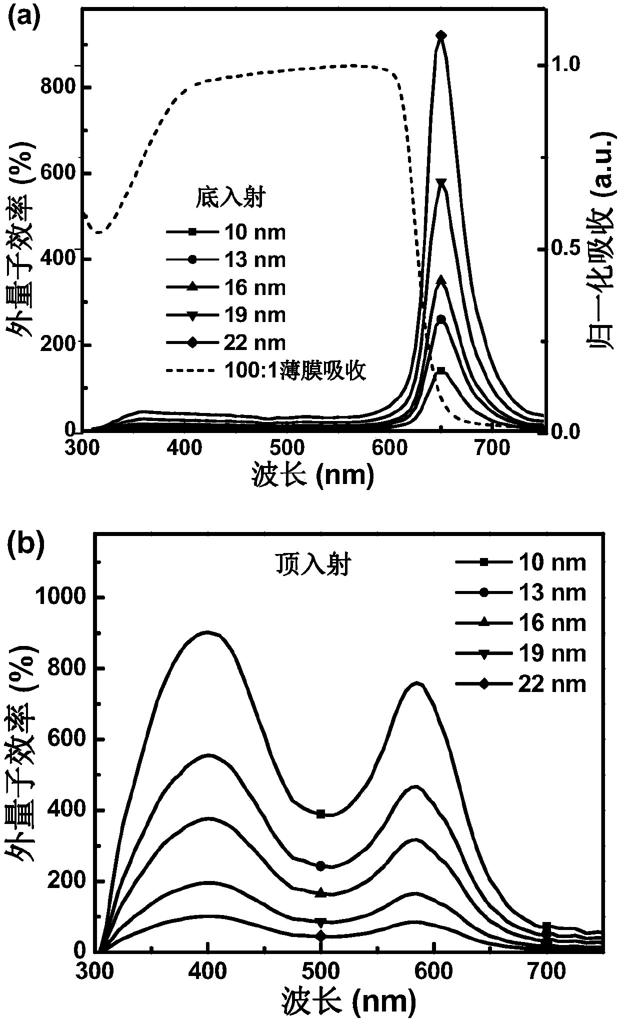
[0058] On the basis of Example 1, the electron donor material of the active layer 4 blended film is selected as P3HT and PTB7-Th in a weight ratio of 1:1, and the electron acceptor material is selected from PCBM, and the weight ratio of the electron acceptor remains at 100: 1, such as Figure 6 As shown, the fabricated organic photodetector produces a narrow-band response in the near-infrared band at 790 nanometers under the condition of incident light bottom incidence (ITO side), and the full width at half maximum of the response is less than 30 nanometers, and the top incidence (Al side) Under normal circumstances, a broadband response is generated in the range of 300-850 nanometers, the full width at half maximum of the response is extended to 500 nanometers, and the response cut-off edge is extended to the near-infrared band. Under bottom / top incidence c
PUM
 Abstract
Description
Claims
Application Information
 - R&D Engineer
- R&D Manager
- IP Professional
- Industry Leading Data Capabilities
- Powerful AI technology
- Patent DNA Extraction
Browse by: Latest US Patents, China's latest patents, Technical Efficacy Thesaurus, Application Domain, Technology Topic.
© 2024 PatSnap. All rights reserved.Legal|Privacy policy|Modern Slavery Act Transparency Statement|Sitemap