AR glasses
A technology of AR glasses and solar cells, applied in the field of AR glasses, can solve the problems of reducing the convenience of AR glasses, affecting the comfort of users, limiting the application range, etc., and achieving the effects of simple structure, reduced weight, and extended battery life
- Summary
- Abstract
- Description
- Claims
- Application Information
AI Technical Summary
Benefits of technology
Problems solved by technology
Method used
Image

Examples
Embodiment 1
[0027] see image 3 As shown, the manufacturing process of the AR glasses 100 is as follows:
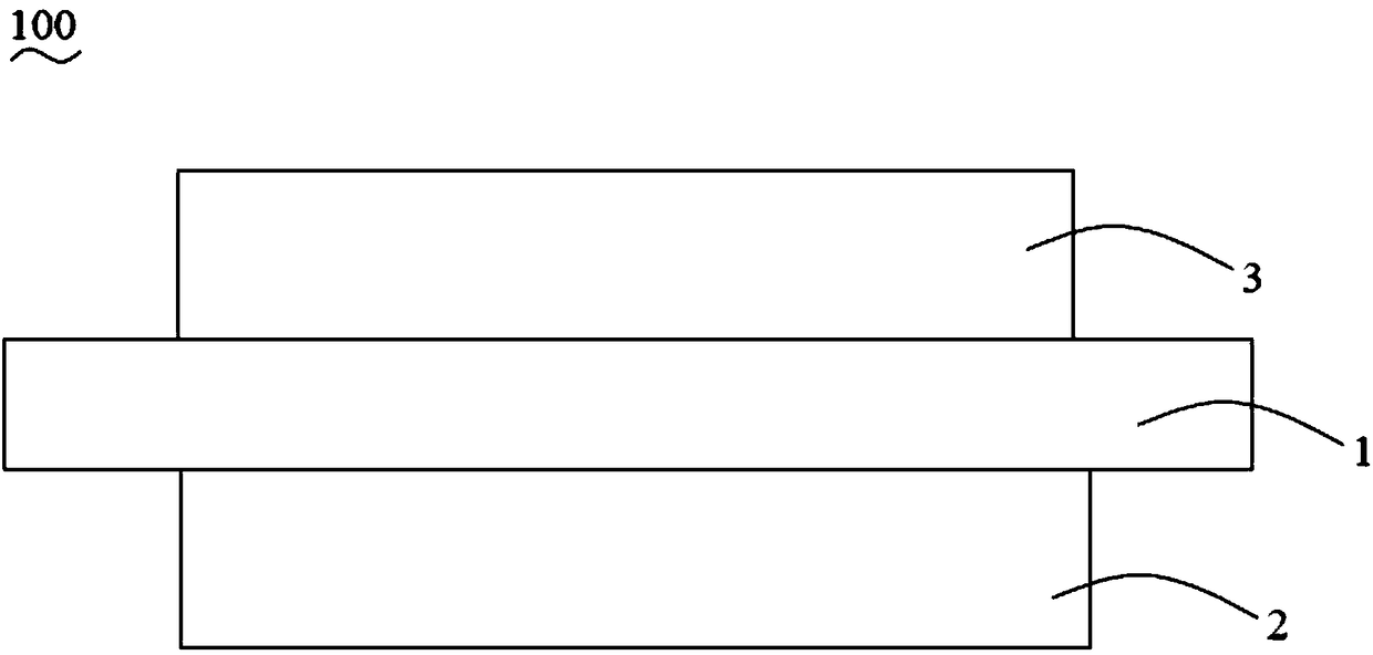
[0028] S101, providing the silicon substrate 1 having opposite sides;
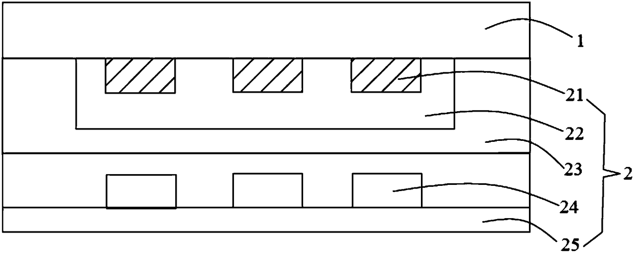
[0029] S201, using a magnetron sputtering method to form the anode 21 of the micro OLED on one side of the silicon substrate 1;
[0030] S301, forming an organic material layer of the micro OLED and a cathode of the micro OLED by evaporation on the anode 21 of the micro OLED;
[0031] S401. Encapsulate the anode 21, the organic material layer, and the cathode of the micro OLED by using a thin film encapsulation process to form the encapsulation layer 23;
[0032] S501, providing the package cover plate 25 and the color filter 24, and aligning the package cover plate 25 and the color filter 24 with the package layer 23 through a photoresist to form a The display function layer 2 is a micro OLED device;
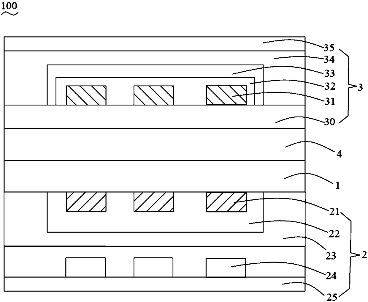
[0033] S601, providing a flexible base layer 30, using a magnetron sputtering method to form the anode 31 of t
Embodiment 2
[0038] see Figure 4 As shown, the manufacturing process of the AR glasses 100 is as follows:
[0039] S101, providing the silicon substrate 1 having opposite sides;
[0040] S201, using a magnetron sputtering method to form the anode 21 of the micro OLED on one side of the silicon substrate 1;
[0041] S301, forming an organic material layer of the micro OLED and a cathode of the micro OLED by evaporation on the anode 21 of the micro OLED;
[0042] S401. Encapsulate the anode 21, the organic material layer, and the cathode of the micro OLED by using a thin film encapsulation process to form the encapsulation layer 23;
[0043] S502, providing the package cover 25 and the color filter 24, and aligning and bonding the package cover 25 and the color filter 24 to the package layer 23 through photoresist to form The display function layer 2;
[0044] S602, using a magnetron sputtering method to form the anode 31 of the solar cell on the side of the silicon substrate 1 away from t
PUM
 Abstract
Description
Claims
Application Information
 - R&D Engineer
- R&D Manager
- IP Professional
- Industry Leading Data Capabilities
- Powerful AI technology
- Patent DNA Extraction
Browse by: Latest US Patents, China's latest patents, Technical Efficacy Thesaurus, Application Domain, Technology Topic.
© 2024 PatSnap. All rights reserved.Legal|Privacy policy|Modern Slavery Act Transparency Statement|Sitemap