MOS transistor switch, preparation method thereof and electronic device comprising the same
A technology of MOS transistors and switches is applied in the field of preparation of trench MOS devices, which can solve the problems of high cost and complicated preparation process, and achieve the effect of reducing cost and reducing photolithography process.
- Summary
- Abstract
- Description
- Claims
- Application Information
AI Technical Summary
Problems solved by technology
Method used
Image

Examples
Example Embodiment
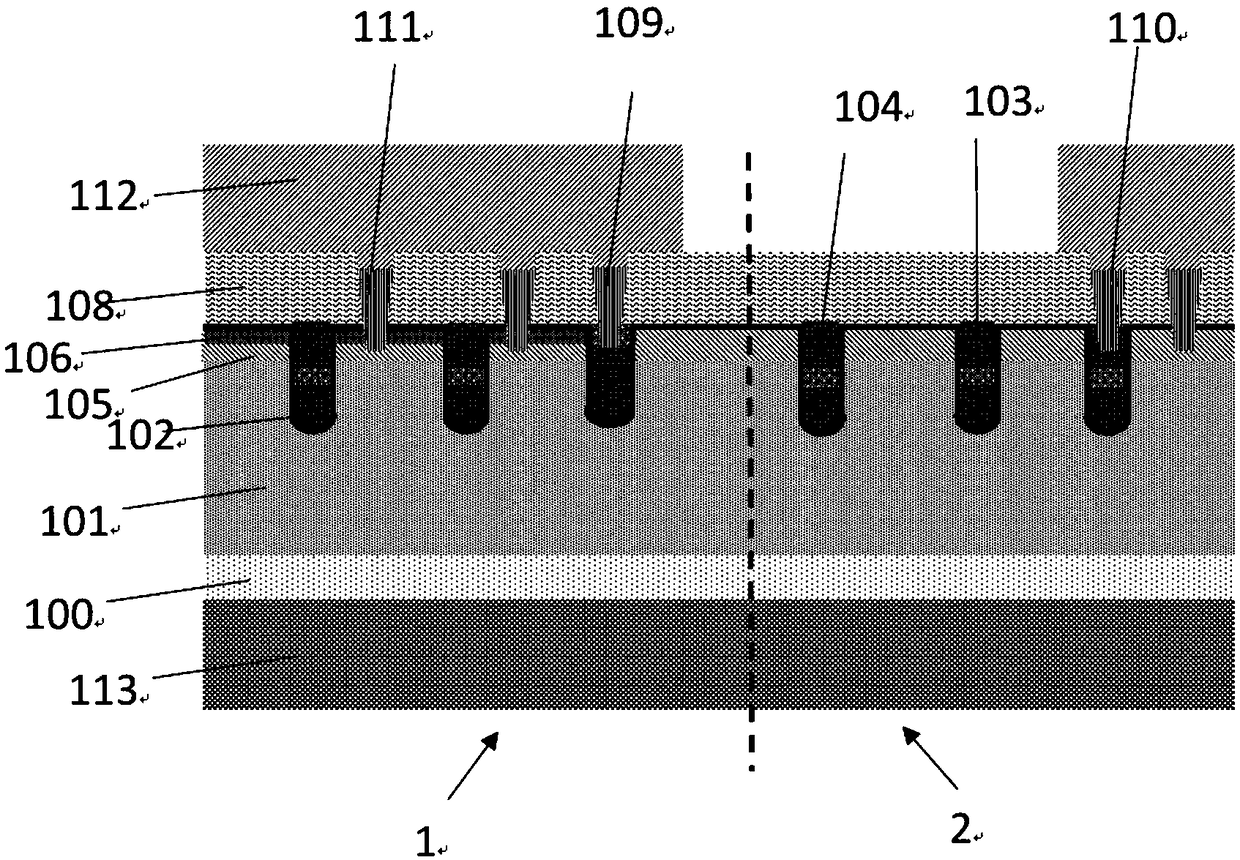
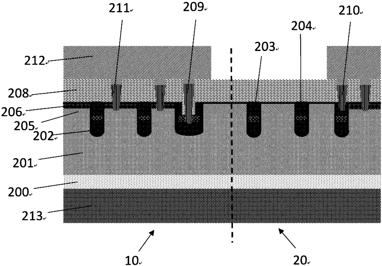
[0045] The first embodiment of the present invention relates to a MOS transistor switch (such as figure 2 Shown), which is prepared on the substrate 200, the trenches in the epitaxial layer 201 are divided into two types, the first trench 2011 and the second trench 2012, the width of the second trench 2012 is larger than that of the first trench 2011, the first trench is filled with the first gate 202 and the second gate 204, the first gate 202 and the second gate 204 are separated by the gate interlayer dielectric layer 203, and the second trench 2012 The first gate 202 is filled, and the first gate metal 209 is drawn from the first gate in the second trench. By setting the trench with two different widths, the first gate metal is drawn from the first gate of the trench with a larger width, which makes the fabrication of the transistor easier.
[0046] The width and depth of the first trench and the second trench can be designed according to requirements. In a specific embodiment,
PUM
| Property | Measurement | Unit |
|---|---|---|
| Width | aaaaa | aaaaa |
| Width | aaaaa | aaaaa |
Abstract
Description
Claims
Application Information
 - R&D Engineer
- R&D Manager
- IP Professional
- Industry Leading Data Capabilities
- Powerful AI technology
- Patent DNA Extraction
Browse by: Latest US Patents, China's latest patents, Technical Efficacy Thesaurus, Application Domain, Technology Topic.
© 2024 PatSnap. All rights reserved.Legal|Privacy policy|Modern Slavery Act Transparency Statement|Sitemap