Novel surface acoustic wave or transverse wave exciter acoustic-microwave device chip structure

A technology of surface acoustic wave and chip structure, which is applied to device components, piezoelectric devices/electrostrictive devices, electrical components, etc., and can solve the problems of reduced sensitivity and anti-interference ability, large acoustic wave transmission loss, and large acoustic wave loss. , to achieve the effect of reducing transmission loss and microwave insertion loss, improving frequency and quality factor and other performance effects

Pending Publication Date: 2019-03-01
INST OF ELECTRICAL ENG CHINESE ACAD OF SCI +1
View PDF0 Cites 2 Cited by
  • Summary
  • Abstract
  • Description
  • Claims
  • Application Information

AI Technical Summary

Benefits of technology

This new design for an ultrasonic device has two technical features that improve its efficiency at transmitting sound waves through materials like air (or water) media. Firstly it introduces a special type called surface acousto-wave mode which can be used instead of traditional methods such as vibrating metal plates. Secondly by filling certain areas between different types of crystals, this technology allows for better control over how much energy they transmit when compared to regular devices made from solid metallics. Overall, these improvements lead to improved overall functionality and reduced power consumption during operation.

Problems solved by technology

This patented describes different ways to make better electronic components with less energy usage while maintaining good electrical properties like resistance or impedence. These techniques include replacing expensive metallic surfaces with carbon nanotubbles instead of gold plates, which helps decrease interferivity between signals and enhances device efficiency. Additionally, exploring alternative methods involving diamonds and graphene layers has become possible due to its superior mechanical strength compared to pure ceramics.

Method used


Image

  • Novel surface acoustic wave or transverse wave exciter acoustic-microwave device chip structure
  • Novel surface acoustic wave or transverse wave exciter acoustic-microwave device chip structure
  • Novel surface acoustic wave or transverse wave exciter acoustic-microwave device chip structure

Examples


Embodiment Construction

[0026] The following will clearly and completely describe the technical solutions in the embodiments of the present invention with reference to the accompanying drawings in the embodiments of the present invention. Obviously, the described embodiments are only some, not all, embodiments of the present invention. Based on the embodiments of the present invention, all other embodiments obtained by persons of ordinary skill in the art without making creative efforts belong to the protection scope of the present invention.

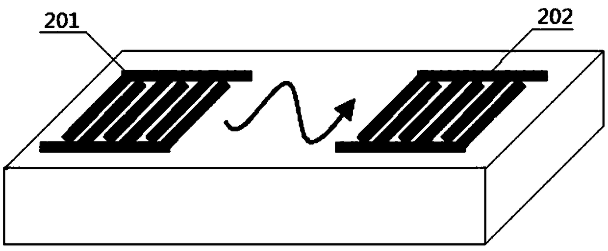
[0027] The purpose of the present invention is to provide a new surface acoustic wave or shear wave excited bulk acoustic wave microwave device chip structure, which reduces the transmission loss and microwave insertion loss of the device, and improves the performance of the device such as frequency and quality factor.

[0028] In order to make the above objects, features and advantages of the present invention more comprehensible, the present invention will be fu


PUM


Abstract

The invention discloses a novel surface acoustic wave or transverse wave exciter acoustic-microwave device chip structure. The chip structure comprises a surface acoustic wave or transverse wave exciter acoustic-microwave device chip circuit and a chip substrate; a first groove and a second groove are arranged in the chip substrate; a first piezoelectric material is filled in the first groove; a first electrode is arranged on the first piezoelectric material; one end of the first electrode is connected with the first piezoelectric material; the other end of the first electrode is connected with the signal input end of the chip circuit; a second piezoelectric material is filled in the second groove; a second electrode is arranged on the second piezoelectric material; one end of the second electrode is connected with the second piezoelectric material; and the other end of the second electrode is connected with the signal output end of the chip circuit. By means of the novel surface acoustic wave or transverse wave exciter acoustic-microwave device chip structure provided in the invention, the transmission loss and microwave insertion loss of the device can be reduced; and the performances of the device, such as the frequency and the quality factor, can be improved.

Description


Claims


Application Information

Patent Timeline
Owner INST OF ELECTRICAL ENG CHINESE ACAD OF SCI
Why Eureka
Try Eureka