Fabrication method of display panel, display panel and display device
A display panel and display area technology, applied in nonlinear optics, instruments, optics, etc., can solve the problem of large frame of the display panel
- Summary
- Abstract
- Description
- Claims
- Application Information
AI Technical Summary
Problems solved by technology
Method used
Image

Examples
Embodiment Construction
[0038] In order to make the above objects, features and advantages of the present invention more comprehensible, the present invention will be further described in detail below in conjunction with the accompanying drawings and specific embodiments.
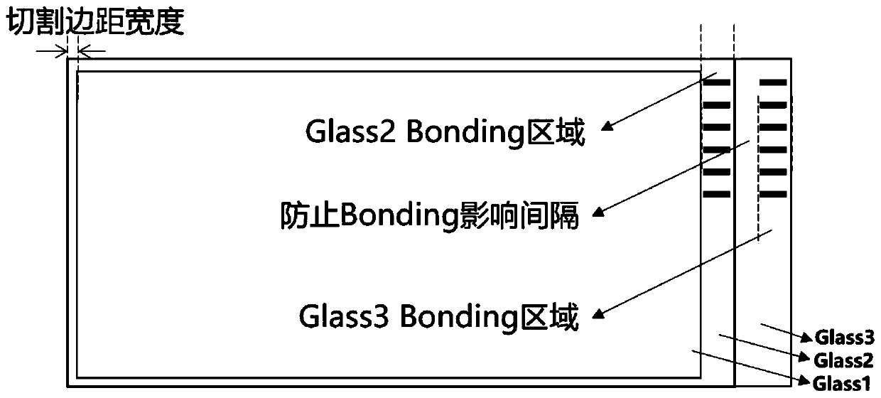
[0039] The inventors found that, with reference to figure 1 , in the related art, the upper bonding area and the lower bonding area are located at the same end of the display panel. Since the upper bonding IC etc. are bent upward, a certain horizontal size will be occupied, and at the same time, in order to avoid the temperature between the two bonding areas Due to the interaction with the pressure, a gap area (about 5mm) needs to be set between the lower bonding area and the upper bonding area, resulting in a large frame of the display panel and high process requirements.
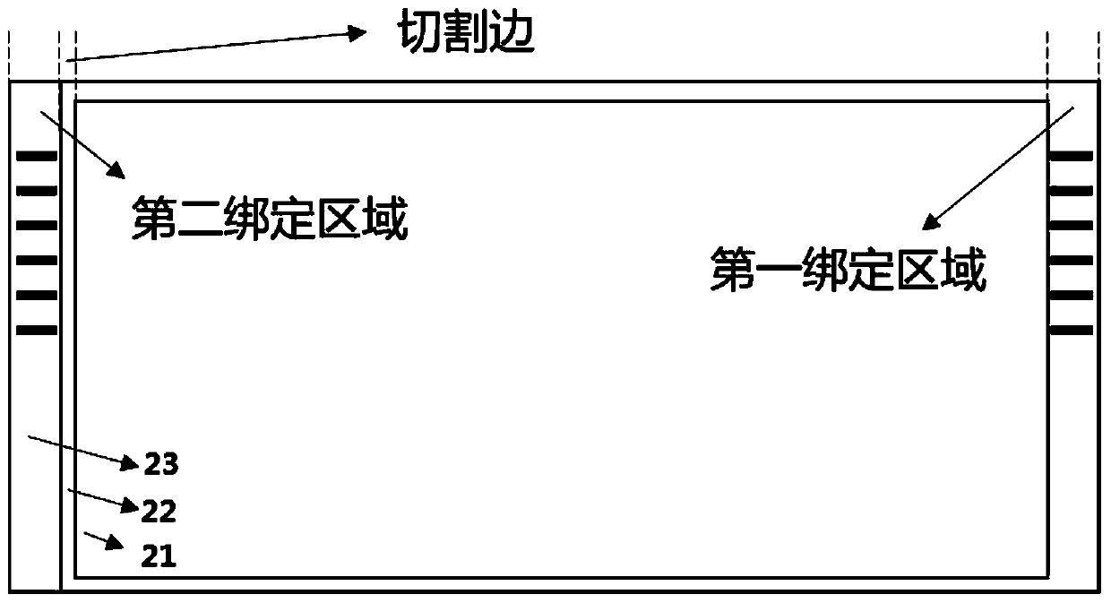
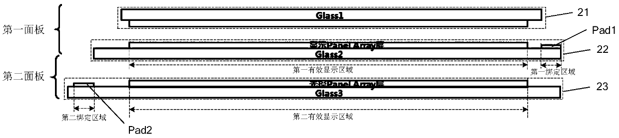
[0040] In order to solve this problem, an embodiment of the present application provides a display panel, referring to figure 2 with image 3 , the display pa
PUM
| Property | Measurement | Unit |
|---|---|---|
| Width | aaaaa | aaaaa |
Abstract
Description
Claims
Application Information
 - R&D Engineer
- R&D Manager
- IP Professional
- Industry Leading Data Capabilities
- Powerful AI technology
- Patent DNA Extraction
Browse by: Latest US Patents, China's latest patents, Technical Efficacy Thesaurus, Application Domain, Technology Topic.
© 2024 PatSnap. All rights reserved.Legal|Privacy policy|Modern Slavery Act Transparency Statement|Sitemap