Flash chip and reading method thereof
A chip and reading circuit technology, applied in the field of memory, can solve the problems of high power consumption and abnormal system operation, and achieve the effect of strong practicability and novel design
- Summary
- Abstract
- Description
- Claims
- Application Information
AI Technical Summary
Problems solved by technology
Method used
Image

Examples
Example Embodiment
[0016] In order to make the technical purpose, technical solutions and technical effects of the present invention clearer and facilitate those skilled in the art to understand and implement the present invention, the present invention will be further described in detail below with reference to the accompanying drawings and specific embodiments.
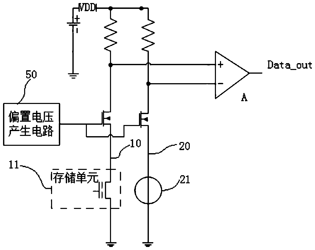
[0017] like figure 1 shown, figure 1 A circuit diagram of a read circuit is shown. The working principle of the read circuit is as follows: the inverting input terminal of the comparator A is connected to the reference current branch 20, and the non-inverting input terminal of the comparator A is connected to the memory cell branch 10; if the memory cell is a programming memory cell (pgm cell), it is turned on The voltage (VTH) is high, and there is no current in the memory cell at this time, and the voltage of the non-inverting input terminal of comparator A is higher than the voltage of the inverting input terminal of comparator A; if
PUM
 Abstract
Description
Claims
Application Information
 - R&D Engineer
- R&D Manager
- IP Professional
- Industry Leading Data Capabilities
- Powerful AI technology
- Patent DNA Extraction
Browse by: Latest US Patents, China's latest patents, Technical Efficacy Thesaurus, Application Domain, Technology Topic.
© 2024 PatSnap. All rights reserved.Legal|Privacy policy|Modern Slavery Act Transparency Statement|Sitemap