Preparation method and application of wafer-level absolute single-layer transition metal chalcogenide
A technology of transition metal chalcogenides and transition metals, which is applied in the direction of metal material coating process, coating, gaseous chemical plating, etc., can solve the problem that it is difficult to directly obtain single-layer two-dimensional transition metal chalcogenide crystals, etc., to achieve Excellent photoelectric properties, high crystal quality, and large single crystal size
- Summary
- Abstract
- Description
- Claims
- Application Information
AI Technical Summary
Benefits of technology
Problems solved by technology
Method used
Image

Examples
Embodiment 1
[0096] This embodiment provides an absolute single-layer WS 2 The preparation method specifically comprises the following steps:
[0097] A method for preparing transition metal chalcogenides by combining a monodisperse metal source and a CVD method. The chemical vapor deposition device is a device known in the art. The chemical vapor deposition device used in this embodiment includes a single temperature zone tube furnace, A quartz tube, wherein the quartz tube is 1.4 m long and 1 inch in diameter.
[0098] The method comprises the steps of:
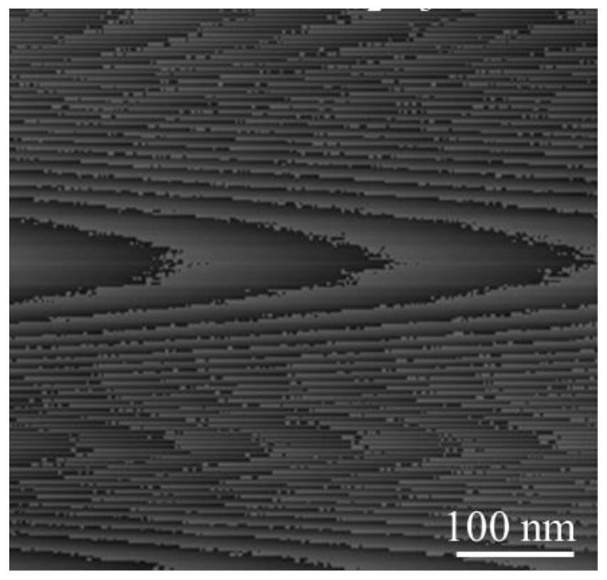
[0099] (1) Take a commercially available C-face sapphire substrate (purchased from Suzhou Yancai Micro-Nano Technology Co., Ltd.) (the atomic force microscope characterization of the unannealed sapphire substrate is as follows Figure 1a shown), cut into small pieces of 1cm×1cm, ultrasonically cleaned with acetone, absolute ethanol, and deionized water for 10 minutes each to obtain a substrate with a clean surface, annealed in a muffle fu
Embodiment 2
[0106] This embodiment provides an absolute single-layer MoS 2 The preparation method of described monodisperse substrate preparation device and chemical vapor deposition device are identical with embodiment 1, and the difference of described method and embodiment 1 is:
[0107] In step (2), 0.006181 g of ammonium molybdate (purchased from Aladdin Reagents) was weighed, dissolved in a mixed solvent of 4 mL of deionized water and 6 mL of absolute ethanol, and heated and stirred at 90°C for 1 h.
Embodiment 3
[0109] This embodiment provides an absolute single-layer MoSe 2 The preparation method of described monodisperse substrate preparation device and chemical vapor deposition device are identical with embodiment 1, and the difference of described method and embodiment 1 is:
[0110] In step (2), 0.006181g of ammonium molybdate (purchased from Aladdin Reagents) needs to be weighed, dissolved in a mixed solvent of 4mL deionized water and 6mL absolute ethanol, heated and stirred at 90°C for 1h;
[0111] Step (5) is to place 80mg of Se powder and the substrate obtained in step (4) successively in a quartz tube with a diameter of 1 inch according to the airflow direction, and the distance between the sapphire substrate and the Se powder is 18cm, wherein the sapphire substrate is placed in the tube The location of the central temperature zone of the furnace;
[0112] In step (6), heating is performed until the temperature of the place where the sapphire substrate is placed reaches 900° C
PUM
| Property | Measurement | Unit |
|---|---|---|
| Horizontal size | aaaaa | aaaaa |
| Carrier mobility | aaaaa | aaaaa |
| Horizontal size | aaaaa | aaaaa |
Abstract
Description
Claims
Application Information
 - R&D Engineer
- R&D Manager
- IP Professional
- Industry Leading Data Capabilities
- Powerful AI technology
- Patent DNA Extraction
Browse by: Latest US Patents, China's latest patents, Technical Efficacy Thesaurus, Application Domain, Technology Topic.
© 2024 PatSnap. All rights reserved.Legal|Privacy policy|Modern Slavery Act Transparency Statement|Sitemap