Edge-emitting semiconductor laser chip testing method and system
A chip testing and semiconductor technology, applied in the direction of electronic circuit testing, instruments, measuring electronics, etc., can solve problems affecting production efficiency, high production cost of equipment, large equipment footprint, etc., to reduce handling time, improve testing efficiency, The effect of reducing the footprint
- Summary
- Abstract
- Description
- Claims
- Application Information
AI Technical Summary
Problems solved by technology
Method used
Image

Examples
Example Embodiment
[0029] Next, the technical solutions in the embodiments of the present invention will be described in connection with the drawings of the embodiments of the present invention, and it is understood that the described embodiments are merely the embodiments of the present invention, not all of the embodiments. Based on the embodiments of the present invention, those of ordinary skill in the art will belong to the scope of the present invention in the scope of the present invention without making creative labor premises.
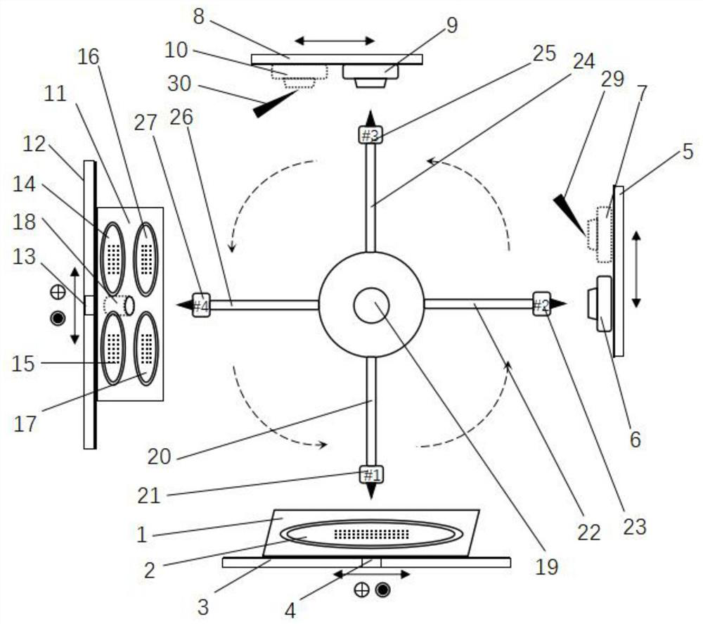
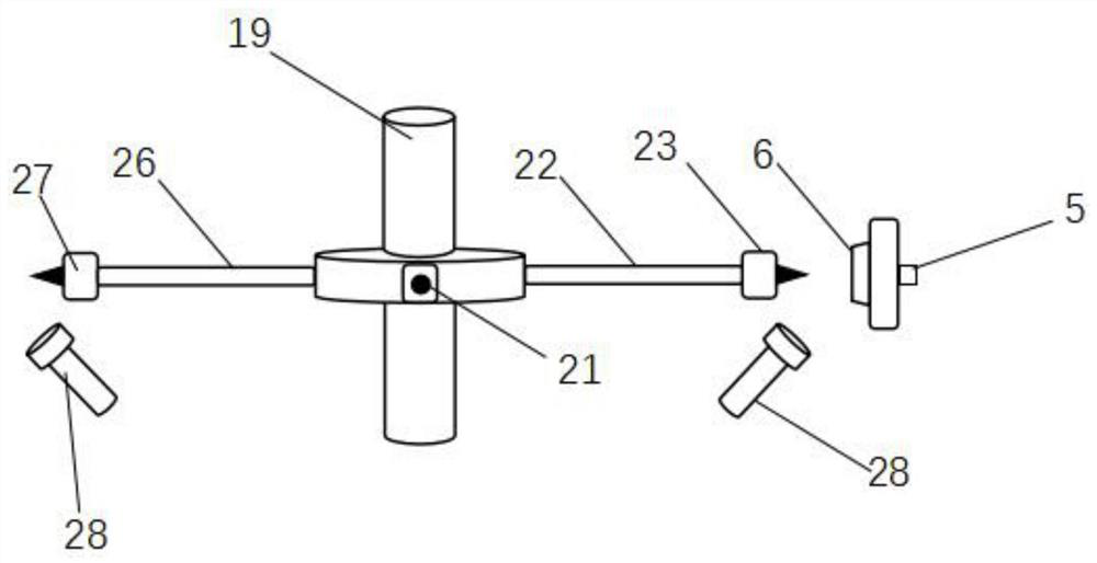
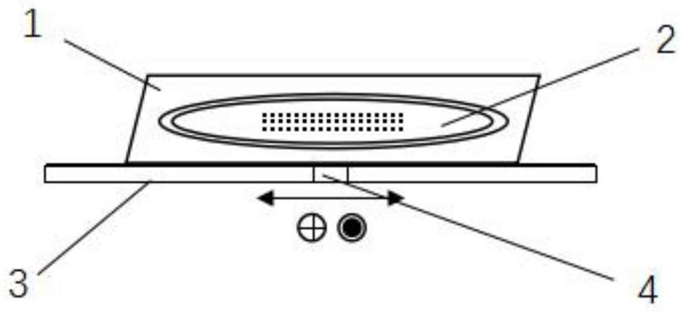
[0030] See Figure 1 to 6, Embodiments provide a mechanism for feeding the edge-emitting semiconductor laser chip test system, comprising a feeding zone, a lower zone, a test zone and a reclaiming mechanism, said test zone comprising a plurality of test stage, the present invention includes a plurality of take and a reclaimer for driving each head of the pick head rotating shaft 19, the upper feed zone, the lower feed zone of each of the test stage and encircling the sh
PUM
 Abstract
Description
Claims
Application Information
 - R&D Engineer
- R&D Manager
- IP Professional
- Industry Leading Data Capabilities
- Powerful AI technology
- Patent DNA Extraction
Browse by: Latest US Patents, China's latest patents, Technical Efficacy Thesaurus, Application Domain, Technology Topic.
© 2024 PatSnap. All rights reserved.Legal|Privacy policy|Modern Slavery Act Transparency Statement|Sitemap