Touch screen and manufacturing method
A touch screen and circuit technology, which is applied in the direction of instruments, electrical digital data processing, data processing input/output process, etc., can solve the problems of high production cost, many layers, complex production process, etc., and achieve saving of manufacturing cost, The effect of simple processing technology and simplified product structure
- Summary
- Abstract
- Description
- Claims
- Application Information
AI Technical Summary
Benefits of technology
Problems solved by technology
Method used
Image

Examples
Embodiment 1
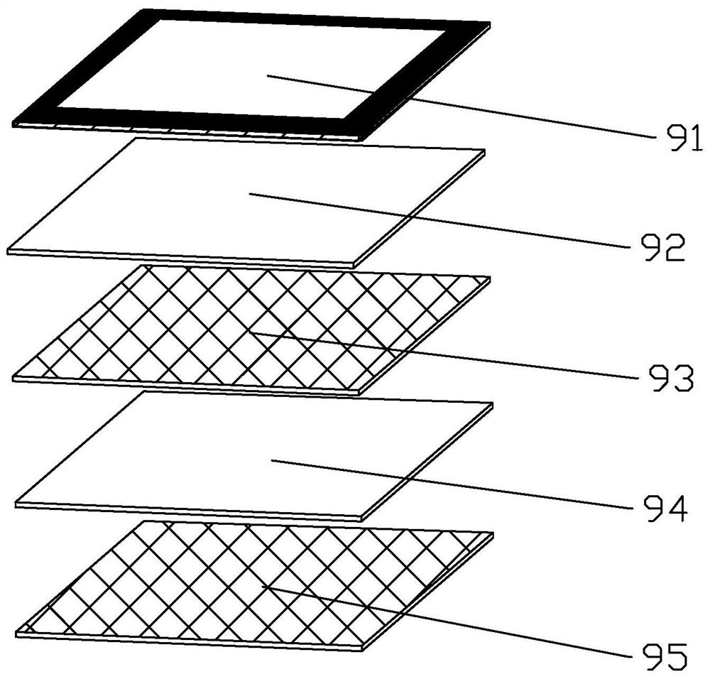
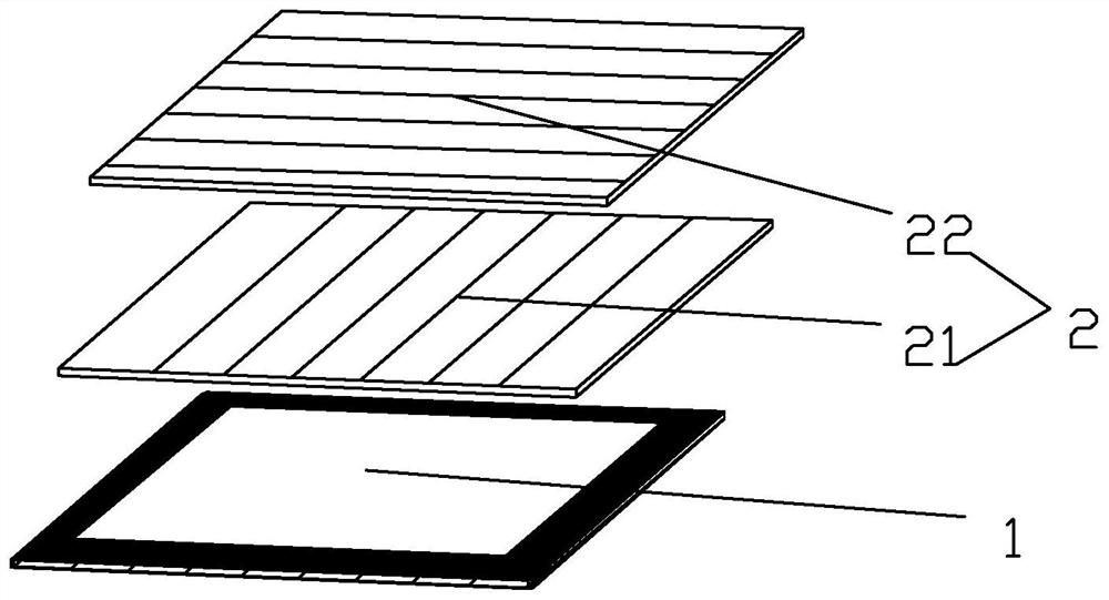
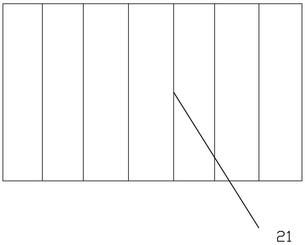
[0041] Such as figure 2 , image 3 and Figure 4 As shown, the touch screen in the present invention includes a glass cover plate 1 and an electrode array 2 solidified on the bonding surface of the glass cover plate 1 through an adhesive layer, and the electrode array 2 includes a conductive RX line 21 and a conductive TX line 22. The projections of the RX line 21 and the TX line 22 in the vertical direction are in a mesh shape and are not connected to each other. Specifically, the adhesive layer includes a first adhesive layer and a second adhesive layer, the first adhesive layer is cured on the bonding surface of the glass cover 1, and the RX circuit 21 is transferred in the first adhesive layer, and the second adhesive layer It is cured on the first adhesive layer and covers the RX circuit 21, and the TX circuit 22 is transferred in the second adhesive layer. Both the first adhesive layer and the second adhesive layer are UV adhesive layers. The function of the UV adhesiv
Embodiment 2
[0045] This embodiment is the manufacturing method of the touch screen in the first embodiment, including the following steps:
[0046] S1. Surface treatment of the glass cover plate: performing light treatment on the glass cover plate 1, and then coating the first adhesive layer on the bonding surface of the glass cover plate 1;
[0047] S2, making RX line mold and TX line mold: according to the designed RX line 21 structure and TX line 22 structure, make RX line 21 mold and TX line 22 mold respectively;
[0048] S3. Transfer printing the RX line structure: After coating the first adhesive layer on the bonding surface of the glass cover plate 1, press the groove on the first adhesive layer through the RX line 21 mold, that is, transfer the RX line 21 structure to the first adhesive layer Above; the first adhesive layer is cured by UV exposure, and forms an integral structure with the glass cover plate 1;
[0049] S4. Transfer the conductive RX circuit: After the RX circuit 21 s
PUM
 Abstract
Description
Claims
Application Information
 - R&D Engineer
- R&D Manager
- IP Professional
- Industry Leading Data Capabilities
- Powerful AI technology
- Patent DNA Extraction
Browse by: Latest US Patents, China's latest patents, Technical Efficacy Thesaurus, Application Domain, Technology Topic.
© 2024 PatSnap. All rights reserved.Legal|Privacy policy|Modern Slavery Act Transparency Statement|Sitemap