Automatic laser repairing method for surface microdefects of large-diameter fused quartz optical element
A technology for laser repair and optical components, applied in the field of engineering optics, can solve problems such as low automation and low efficiency, save time, facilitate analysis, and avoid manual operations.
- Summary
- Abstract
- Description
- Claims
- Application Information
AI Technical Summary
Benefits of technology
Problems solved by technology
Method used
Image

Examples
Embodiment Construction
[0029] In order to enable those skilled in the art to better understand the solutions of the present invention, exemplary implementations or embodiments of the present invention will be described below in conjunction with the accompanying drawings. Apparently, the described embodiments or examples are only part of the embodiments or embodiments of the present invention, not all of them. Based on the implementation modes or examples in the present invention, all other implementation modes or examples obtained by persons of ordinary skill in the art without creative efforts shall fall within the protection scope of the present invention.
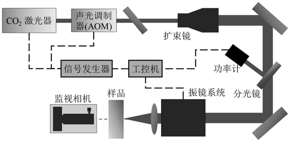
[0030] An embodiment of the present invention provides an automatic laser repair method for micro-defects on the surface of a large-diameter fused silica optical element, the method comprising the following steps:
[0031] Step 1. Obtain the position information and size information of the defect area on the surface of the component;
[0032] St
PUM
 Abstract
Description
Claims
Application Information
 - R&D Engineer
- R&D Manager
- IP Professional
- Industry Leading Data Capabilities
- Powerful AI technology
- Patent DNA Extraction
Browse by: Latest US Patents, China's latest patents, Technical Efficacy Thesaurus, Application Domain, Technology Topic.
© 2024 PatSnap. All rights reserved.Legal|Privacy policy|Modern Slavery Act Transparency Statement|Sitemap