Free layer of magnetic tunnel junction, magnetic tunnel junction and spin transfer torque magnetic random access memory
A magnetic tunnel junction and free technology, applied in the direction of magnetic field controlled resistors, electromagnetic equipment components, material selection, etc., can solve the problems of increasing chip energy consumption, large critical writing current, shortening chip life, etc., to achieve Improve the erasing and writing resistance performance, improve STT efficiency, and reduce the effect of writing current
- Summary
- Abstract
- Description
- Claims
- Application Information
AI Technical Summary
Benefits of technology
Problems solved by technology
Method used
Image

Examples
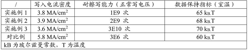
Embodiment 1
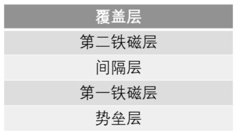
[0032] The free layer provided by this embodiment includes a first ferromagnetic layer, a spacer layer, a second ferromagnetic layer and a capping layer which are deposited in sequence. Wherein, the material of the first ferromagnetic layer is Co-Fe-B alloy (Co accounts for 30wt%, Fe accounts for 50wt%), the thickness is 0.9nm, and the material of the second ferromagnetic layer is Co-Fe alloy (Co accounted for 30wt%), and the thickness was 0.7nm; the spacer layer was composed of W and Mg (W accounted for 40wt%), and the thickness was 0.3nm; the material of the cover layer was Ru, and the thickness was 3nm.
Embodiment 2
[0034] The free layer provided by this embodiment includes a first ferromagnetic layer, a spacer layer, a second ferromagnetic layer and a capping layer which are deposited in sequence. The material of the first ferromagnetic layer is Co-Fe-B alloy (Co accounts for 30wt%, Fe accounts for 50wt%), and the thickness is 0.8nm; the material of the second ferromagnetic layer is Ni-Fe alloy ( Ni accounts for 40 wt %), and the thickness is 0.6 nm; the spacer layer is composed of Ta and Al (Ta accounts for 30 wt %), and the thickness is 0.6 nm; the material of the cover layer is MgO, and the thickness is 2.5 nm.
Embodiment 3
[0036] The free layer provided by this embodiment includes a first ferromagnetic layer, a spacer layer, a second ferromagnetic layer and a capping layer which are deposited in sequence. The material of the first ferromagnetic layer is Co-Fe-Ni alloy (Co accounts for 20wt%, Fe accounts for 60wt%), and the thickness is 0.6nm; the material of the second ferromagnetic layer is Ni-Fe alloy ( Ni accounts for 40 wt%), and the thickness is 0.5 nm; the spacer layer is composed of W and Si (W accounts for 30 wt%), and the thickness is 0.3 nm; the material of the cover layer is MgO, and the thickness is 1.5 nm.
PUM
| Property | Measurement | Unit |
|---|---|---|
| Thickness | aaaaa | aaaaa |
| Thickness | aaaaa | aaaaa |
| Thickness | aaaaa | aaaaa |
Abstract
Description
Claims
Application Information
 - R&D Engineer
- R&D Manager
- IP Professional
- Industry Leading Data Capabilities
- Powerful AI technology
- Patent DNA Extraction
Browse by: Latest US Patents, China's latest patents, Technical Efficacy Thesaurus, Application Domain, Technology Topic.
© 2024 PatSnap. All rights reserved.Legal|Privacy policy|Modern Slavery Act Transparency Statement|Sitemap