Semiconductor memory device with improved saving rate for defective chips
A memory and semiconductor technology, applied in the direction of static memory, digital memory information, information storage, etc., can solve the problems of increased manufacturing cost, chip programming time can not be ignored, etc., to achieve the effect of suppressing the number, suppressing the increase, and improving the recovery rate
- Summary
- Abstract
- Description
- Claims
- Application Information
AI Technical Summary
Problems solved by technology
Method used
Image


Examples
Embodiment 1
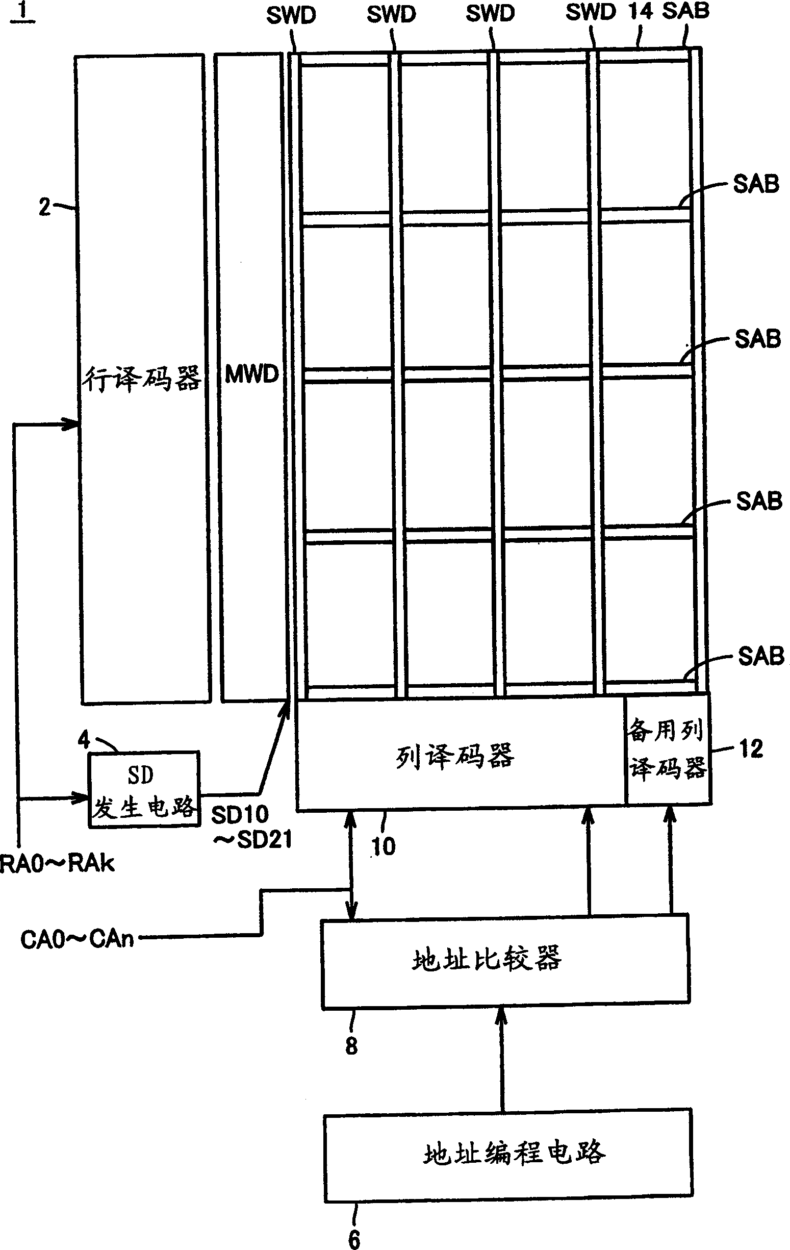
[0045] figure 1 It is a schematic block diagram showing the structure of the semiconductor memory 1 according to the first embodiment of the present invention.
[0046] refer to figure 1 , the semiconductor memory 1 includes: a row decoder 2, which is used to receive row address signals RA0-RAk to select rows of memory cells; a main word driver MWD, which drives the main word line according to the output of the row decoder 2; and SD generation circuit 4 receives row address signals RA0-RAk, and outputs signals SD10-SD21.
[0047] The semiconductor memory 1 also includes: an address programming circuit 6, which stores the address to be replaced corresponding to the defective memory cell in a non-volatile manner; an address comparator 8, which compares the output of the address programming circuit 6 with the column address signals CA0-CAn; The column decoder 10 is used to determine the active state according to the output of the address comparator 8, and selects the column of the
Embodiment 2
[0099] Embodiment 1 relates to an invention for further improving a defect recovery rate when a spare column is provided in a memory cell array. In Embodiment 2, the defect recovery rate can be improved when spare I / O is provided in the memory cell array.
[0100] Figure 8 It is a block diagram showing the structure of the semiconductor memory 201 of the second embodiment.
[0101] refer to Figure 8 , the semiconductor memory 201 includes: an address programming circuit 206, which stores the address of the defective memory cell that is replaced by the spare memory cell; The output of 206 is compared; the SD generation circuit 204 generates signals SD10-SD21 from the row address signal RA and the column address signal CA; and the row decoder+column decoder 202 receives the row address signal RA and the column address signal CA and generates Decode it.
[0102] Since the SD generation circuit 204 has the image 3 The SD generating circuit 4 has the same structure as has be
Embodiment 3
[0132] In the third embodiment, similar to the second embodiment, it relates to the configuration of replacing the spare IO line, but the case where the circuit configuration of the path from the memory cell array to the data input / output terminal is different is described.
[0133] Figure 12 It is a block diagram showing the structure of the semiconductor memory 301 of the third embodiment.
[0134] refer to Figure 12 , the semiconductor memory 301 includes: an address programming circuit 306, which stores the address of the defective memory cell that is replaced by the spare memory cell; The output of 306 is compared; IOS generating circuit 304 receives the output of address comparator 308 and generates signals IOS1~IOS4; and row decoder+column decoder 302 receives row address signal RA and column address signal CA and compares them to decode.
[0135] Semiconductor memory 301 also comprises: main word driver MWD, drives main word line according to the output of row deco
PUM
 Abstract
Description
Claims
Application Information
 - R&D Engineer
- R&D Manager
- IP Professional
- Industry Leading Data Capabilities
- Powerful AI technology
- Patent DNA Extraction
Browse by: Latest US Patents, China's latest patents, Technical Efficacy Thesaurus, Application Domain, Technology Topic.
© 2024 PatSnap. All rights reserved.Legal|Privacy policy|Modern Slavery Act Transparency Statement|Sitemap