Liquid crystal display with double-film transister pixel structure
A liquid crystal display and switching transistor technology, applied in transistors, instruments, optics, etc., can solve problems such as short charging time, line ripple, and change, and achieve the effects of reduced feedthrough voltage, high resolution, and high display frequency
- Summary
- Abstract
- Description
- Claims
- Application Information
AI Technical Summary
Benefits of technology
Problems solved by technology
Method used
Image

Examples
Embodiment Construction
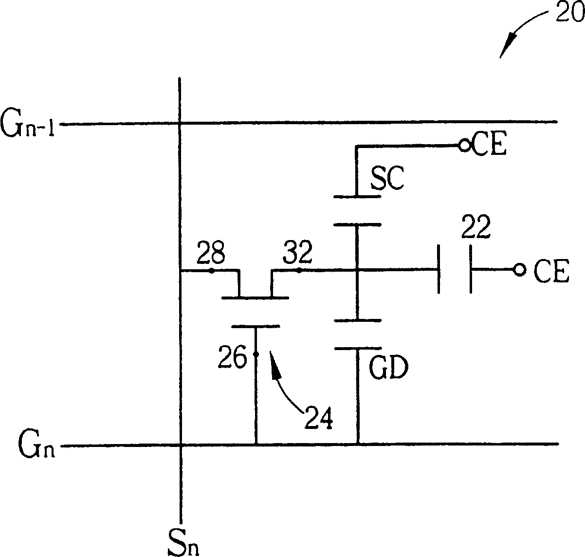
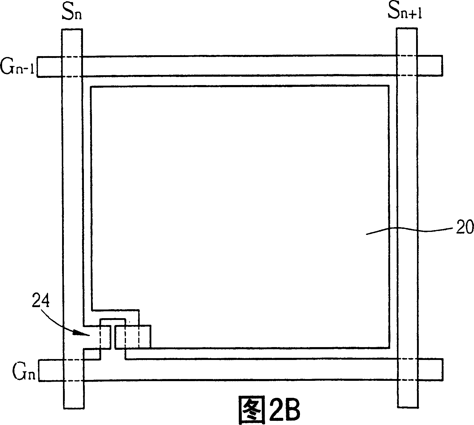
[0024] Please refer to Figure 5, Figure 5A It is a schematic diagram of an equivalent circuit of each pixel 100 of the present invention, and FIG. 5B is a top view of each pixel 100 of the present invention. Such as Figure 5A As shown in FIG. 5B, each pixel 100 of the present invention includes a liquid crystal unit (liquid crystal unit, LC unit) 102 filled with liquid crystal molecules (liquid crystalmolecules, not shown), a pixel electrode (pixel electrode, not shown) , a first thin film transistor (first TFT) 104 and a second thin film transistor (second TFT) 106 . The liquid crystal unit 102 is electrically connected to a common counterelectrode (CE), and the first thin film transistor 104 and the second thin film transistor 106 are both used as switches to control the charging of the pixel electrode (not shown). . Wherein, the gate electrode 108 of the first thin film transistor 104 is electrically connected to the scanning line G of the previous row n-1 , the source 1
PUM
 Abstract
Description
Claims
Application Information
 - R&D Engineer
- R&D Manager
- IP Professional
- Industry Leading Data Capabilities
- Powerful AI technology
- Patent DNA Extraction
Browse by: Latest US Patents, China's latest patents, Technical Efficacy Thesaurus, Application Domain, Technology Topic.
© 2024 PatSnap. All rights reserved.Legal|Privacy policy|Modern Slavery Act Transparency Statement|Sitemap