Method for repairing thin-film transistor array substrate and thin film removing method

A technology for thin film transistors and array substrates, which is applied in the fields of repairing thin film transistor array substrates and removing thin films, can solve the problems of increasing the number of dark spots on the panel, affecting the display quality, etc., so as to improve the process yield and ensure the effect of normal operation.

Active Publication Date: 2007-06-06
AU OPTRONICS CORP
View PDF0 Cites 2 Cited by
  • Summary
  • Abstract
  • Description
  • Claims
  • Application Information

AI Technical Summary

Benefits of technology

The present in this patented technology allows for accurate removal of unwanted material from pixels during production without causing damage caused by excessive heating at certain points within the display device's structure. This results in improved productivity rates while maintaining consistently good quality displays with minimal defects.

Problems solved by technology

This patents discuss how electronic components like cameras require less space than ever before but they now use more powerful computers and smaller screens. To meet these requirements, it becomes necessary to develop lighter and slimmer electronics without sacrificially increasing their overall dimensions. Additionally, while reducing costs, improving efficiency can lead to improved functionality and reduced waste generation during production processes.

Method used


Image

  • Method for repairing thin-film transistor array substrate and thin film removing method
  • Method for repairing thin-film transistor array substrate and thin film removing method
  • Method for repairing thin-film transistor array substrate and thin film removing method

Examples


Embodiment Construction

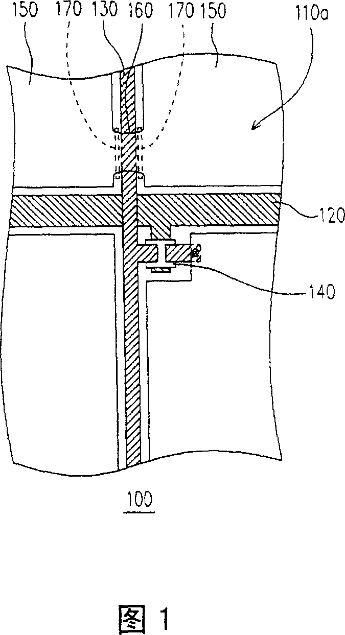
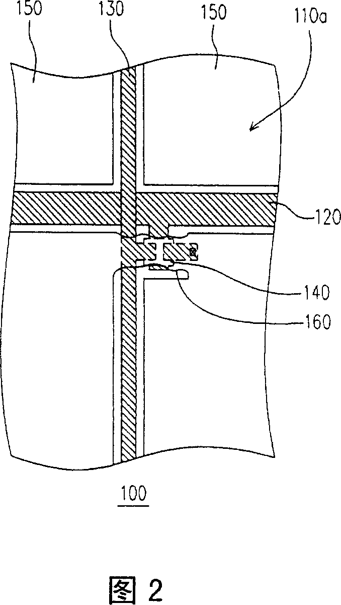
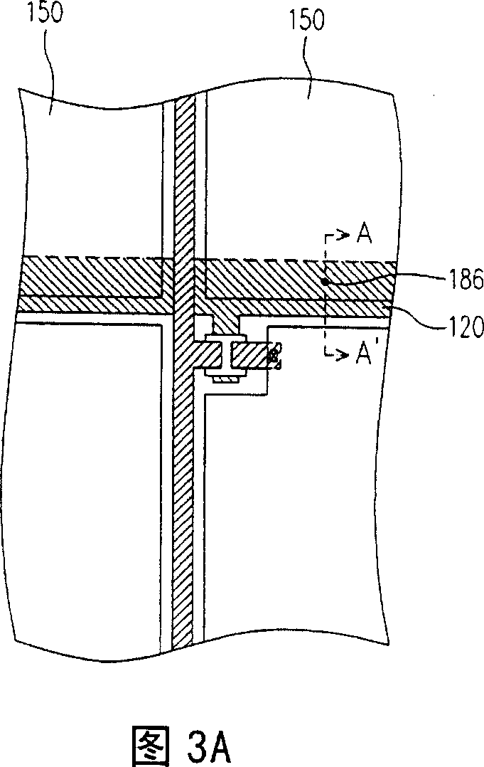
[0030]Please refer to FIG. 1 , which shows a schematic diagram of a thin film transistor array substrate according to a preferred embodiment of the present invention. The thin film transistor array substrate 100 includes, for example, a substrate 110 (shown in FIG. 3B ), a plurality of scanning lines 120 , a plurality of data lines 130 , a plurality of thin film transistors 140 and a plurality of pixel electrodes 150 . Wherein, the scan wires 120 and the data wires 130 are respectively disposed on the substrate 110, and a plurality of pixel regions 110a are divided on the substrate. The thin film transistor 140 is correspondingly disposed in the pixel area 110 a and driven by the scan wiring 120 and the data wiring 130 . In addition, the pixel electrode 150 is correspondingly disposed in the pixel region 110 a and is electrically connected to the corresponding thin film transistor 140 , and the material of the pixel electrode 150 is, for example, a transparent conductive material


PUM

PropertyMeasurementUnit
Pulse widthaaaaaaaaaa
Wavelengthaaaaaaaaaa

Abstract

A method for repairing base plate of thin film transistor array includes exerting a pulse light beam with pulse width of 1/20-1/4 second on residue between pixel electrodes at said base plate in order to remove off at least a partial residue and to make those pixel electrodes at two sides of said residue be electrically insulated.

Description


Claims


Application Information

Patent Timeline
Owner AU OPTRONICS CORP
Why Eureka
Try Eureka