Organometallic precursors, methods of forming a layer using the same and methods of manufacturing semiconductor devices using the same
a technology of organic precursors and semiconductor devices, applied in the field of organic precursors, methods of forming a layer using the same, can solve problems such as damage to the structure of semiconductor devices, and achieve the effect of limiting damage to peripheral structures and/or preventing damag
- Summary
- Abstract
- Description
- Claims
- Application Information
AI Technical Summary
Benefits of technology
Problems solved by technology
Method used
Image
Examples
experimental example 1
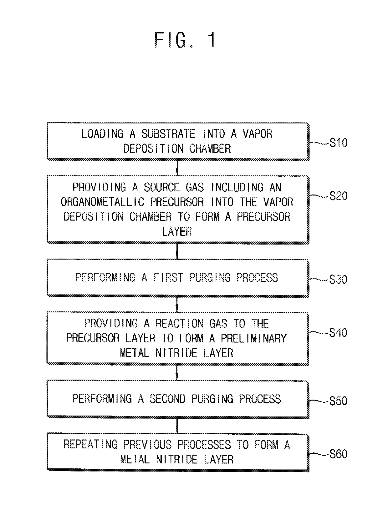
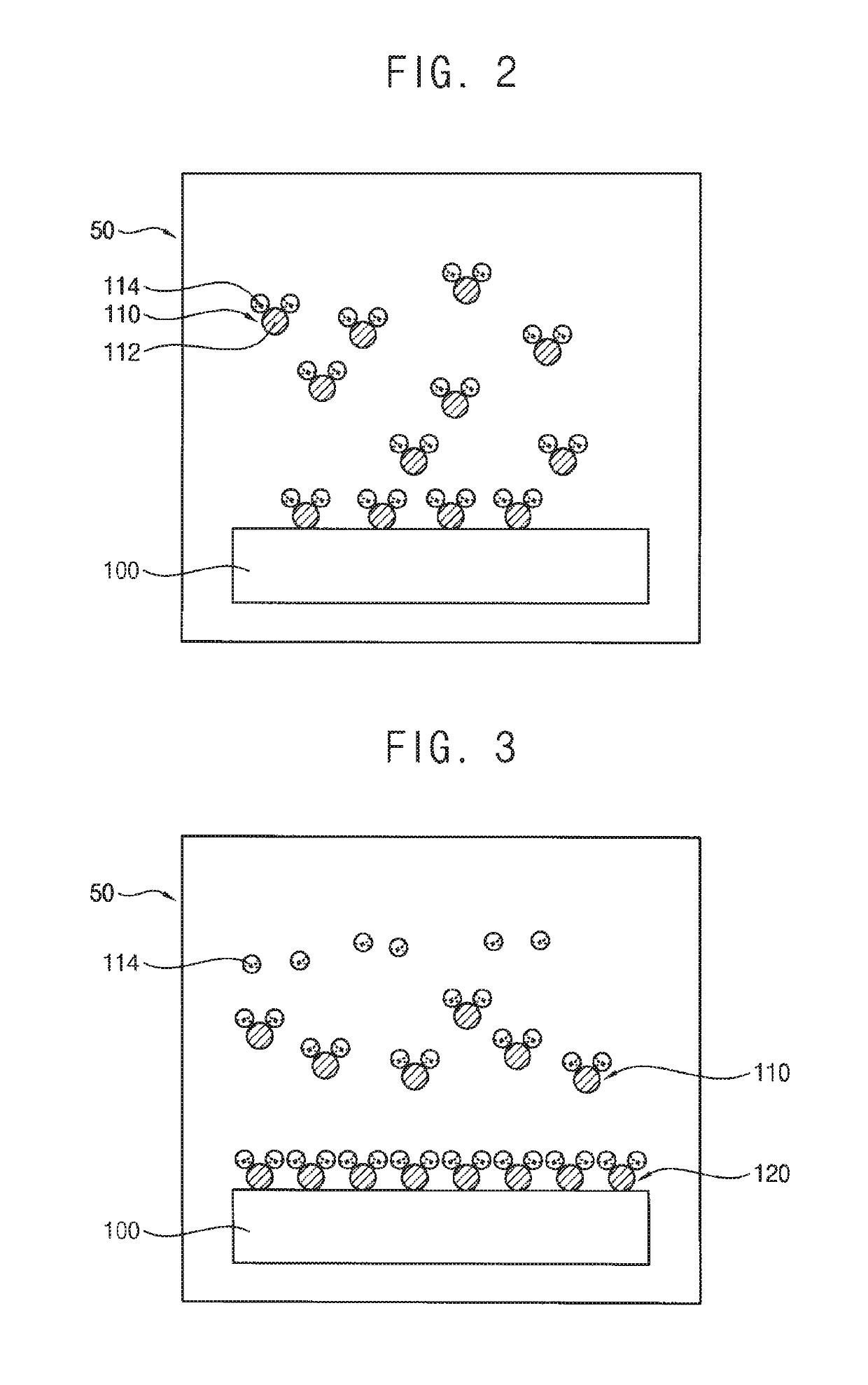
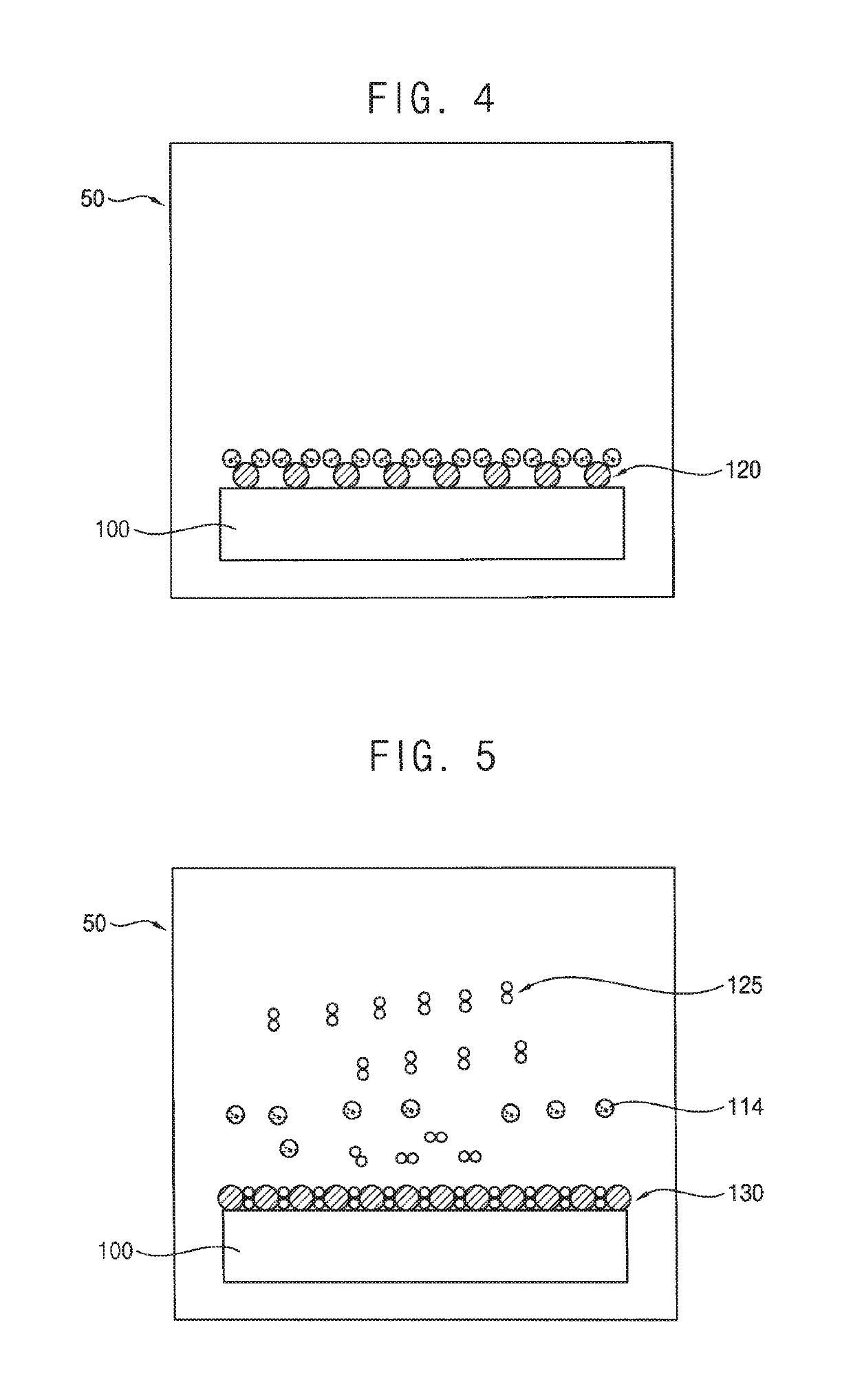
[0188]A silicon substrate was loaded in a vapor deposition chamber for PEALD, a temperature of the substrate was adjusted to be 400° C. (Ethylcyclopentadienyl)(2-methylallyl)(dicarbonyl)tungsten of Synthetic Example 1 was injected as an organometallic precursor from a stainless steel bubbler container, and the temperature was adjusted to be 115° C. The organometallic precursor was provided into the vapor deposition chamber with argon gas as transferring gas (50 sccm) for 15 seconds. Purging was performed with argon gas (1,100 sccm) for 15 seconds to remove byproduct and the organometallic precursor remaining in the vapor deposition chamber. Ammonia gas was injected as reaction gas (2,000 sccm) for 25 seconds to form a tungsten thin film. Thereafter, purging was performed again with argon gas (960 sccm) for 10 seconds to remove byproduct and the reaction gas remaining in the vapor deposition chamber. The above processes were repeated by 300 cycles to form a tungsten-containing thin film
experimental example 2
[0189]A silicon substrate was loaded in a vapor deposition chamber for PEALD, a temperature of the substrate was adjusted to be 250° C. Dimethylpropylsilyl cyclopentadienyl)methyl(tricarbonyl)tungsten of Synthetic Example 2 was injected as an organometallic precursor from a stainless steel bubbler container, and the temperature was adjusted to be 128° C. The organometallic precursor was provided into the vapor deposition chamber with argon gas as transferring gas (50 sccm) for 5 seconds. Purging was performed with argon gas (3,000 sccm) for 10 seconds to remove byproduct and the organometallic precursor remaining in the vapor deposition chamber. Hydrogen gas was injected as reaction gas (500 sccm with RF power 400 W) for 10 seconds to form a tungsten thin film. Thereafter, purging was performed again with argon gas (3,000 sccm) for 10 seconds to remove byproduct and the reaction gas remaining in the vapor deposition chamber. The above processes were repeated by 500 cycles to form a tun
PUM
| Property | Measurement | Unit |
|---|---|---|
| Temperature | aaaaa | aaaaa |
| Temperature | aaaaa | aaaaa |
| Electrical conductor | aaaaa | aaaaa |
Abstract
Description
Claims
Application Information
 - R&D Engineer
- R&D Manager
- IP Professional
- Industry Leading Data Capabilities
- Powerful AI technology
- Patent DNA Extraction
Browse by: Latest US Patents, China's latest patents, Technical Efficacy Thesaurus, Application Domain, Technology Topic.
© 2024 PatSnap. All rights reserved.Legal|Privacy policy|Modern Slavery Act Transparency Statement|Sitemap


