Semiconductor memory device for low power condition

a memory device and semiconductor technology, applied in the field of semiconductor memory devices for low power condition, can solve the problems of increasing the number of semiconductor memory devices that cannot be integrated, the request for supply voltage cannot be achieved, and the difficulty of developing nano-technology, etc., to achieve the effect of reducing power consumption

Inactive Publication Date: 2006-05-04
SK HYNIX INC
View PDF13 Cites 6 Cited by
  • Summary
  • Abstract
  • Description
  • Claims
  • Application Information

AI Technical Summary

Benefits of technology

The technical effect of this patented technology is that it allows for faster operation at lower voltages while reducing energy usage by preventing excessive heat generation during certain operations.

Problems solved by technology

The technical problem addressed in this patent relates to improving the performance of a semiconductor storage device (LD) chip.

Method used


Image

  • Semiconductor memory device for low power condition
  • Semiconductor memory device for low power condition
  • Semiconductor memory device for low power condition

Examples


Embodiment Construction

[0086] Hereinafter, a semiconductor memory device for operating under a low power condition according to the present invention will be described in detail referring to the accompanying drawings.

[0087]FIG. 7 is a block diagram showing a core area of a semiconductor memory device in accordance with an embodiment of the present invention.

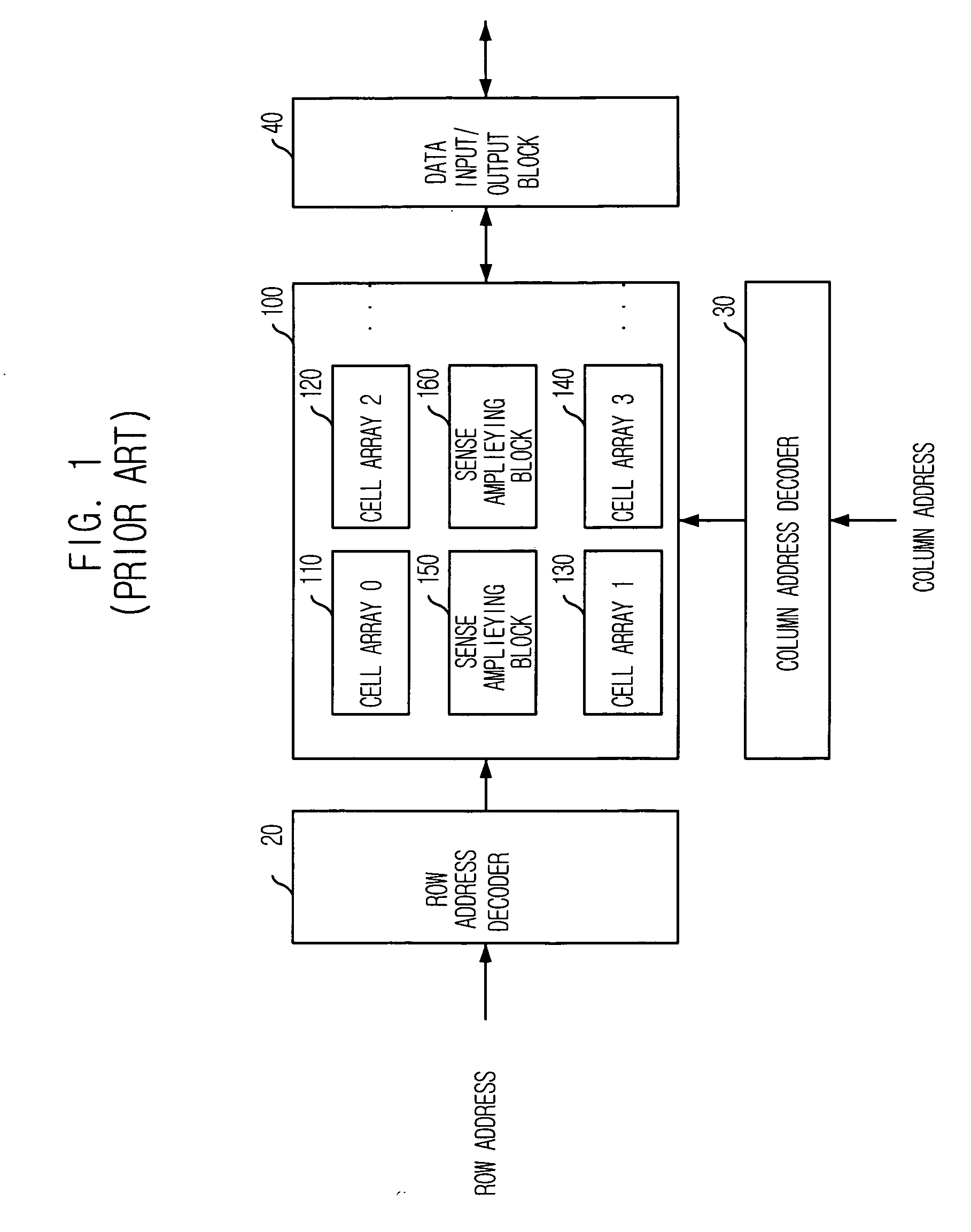
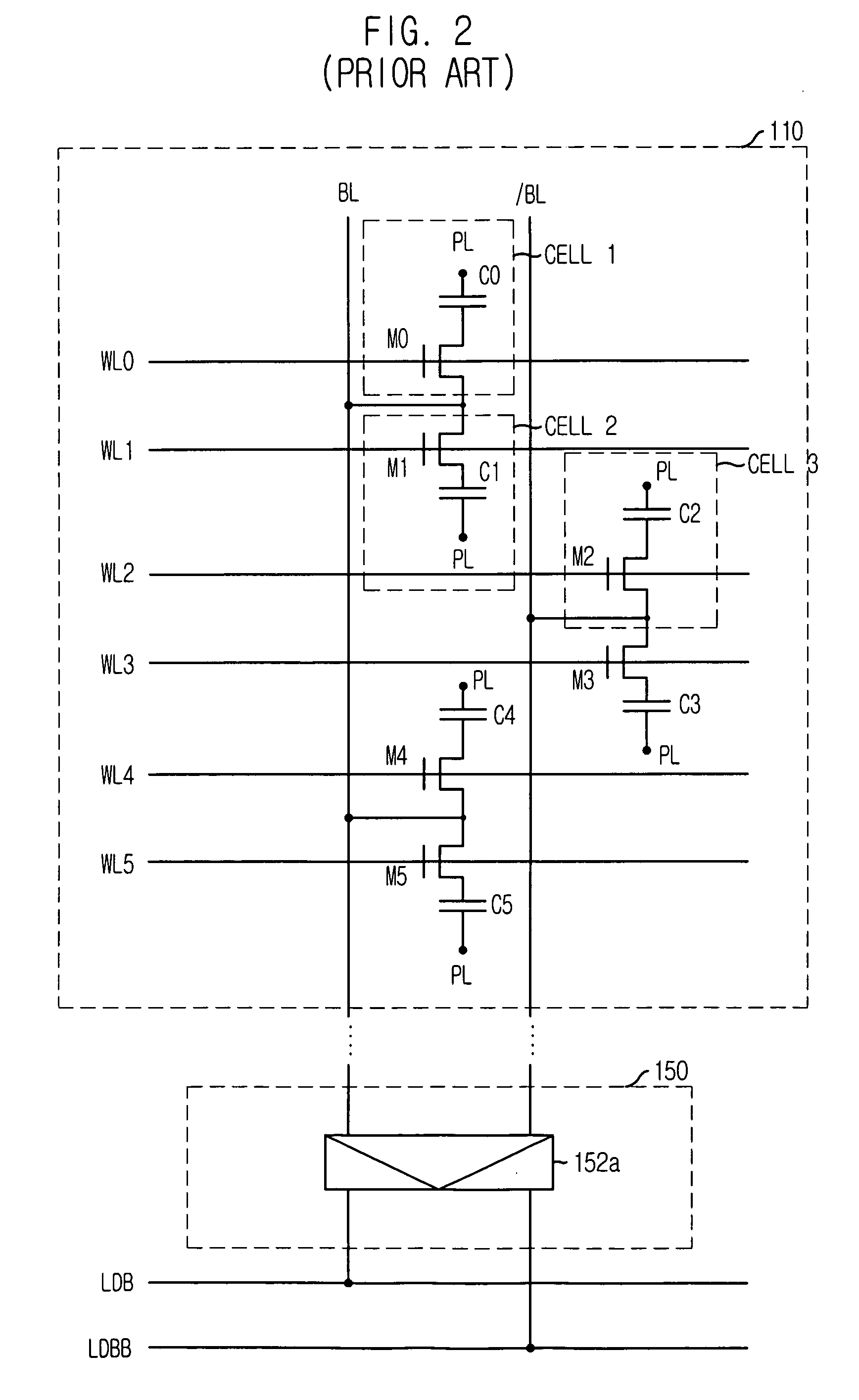
[0088] As shown, the semiconductor memory device includes a first reference cell block 400a, a second reference cell block 400b, a first cell array 300a, a second cell array 300b and a sense amplifying block 200.

[0089] Herein, each cell array, e.g., 300a, includes a plurality of unit cells, each for storing a data and outputting the data to one of a bit line and a bit line bar in response to inputted address and command; and the sense amplifying block 200 is for sensing and amplifying data outputted from each cell array. The first cell array 300a is coupled to the sense amplifying block 200 through a plurality of bit lines, e.g., BLn and BLn+1. The sec


PUM


Abstract

A semiconductor memory device for reading or writing data from or to a memory cell includes at least one cell array having a plurality of memory cells for outputting a stored data to one of a bit line and a bit line bar in response to inputted address and command; at least one reference cell array for outputting a reference signal to the other of the bit line and the bit line bar; a precharge block for precharging the bit line and the bit line bar as a ground; and a sense amplifying block for sensing and amplifying the data by using a core voltage for operating the semiconductor memory device and a high voltage having a higher voltage level than the core voltage.

Description


Claims


Application Information

Patent Timeline
Owner SK HYNIX INC
Why Eureka
Try Eureka