Semiconductor on glass insulator with deposited barrier layer
a technology of glass insulator and glass insulator, which is applied in the direction of semiconductor/solid-state device manufacturing, basic electric elements, electric devices, etc., can solve the problems of cost and/or bond strength and durability, cost of silicon wafer, and cost of support substra
- Summary
- Abstract
- Description
- Claims
- Application Information
AI Technical Summary
Benefits of technology
Problems solved by technology
Method used
Image

Examples
example 1
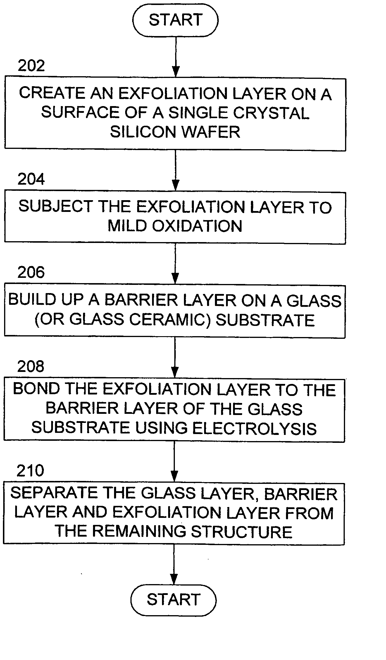
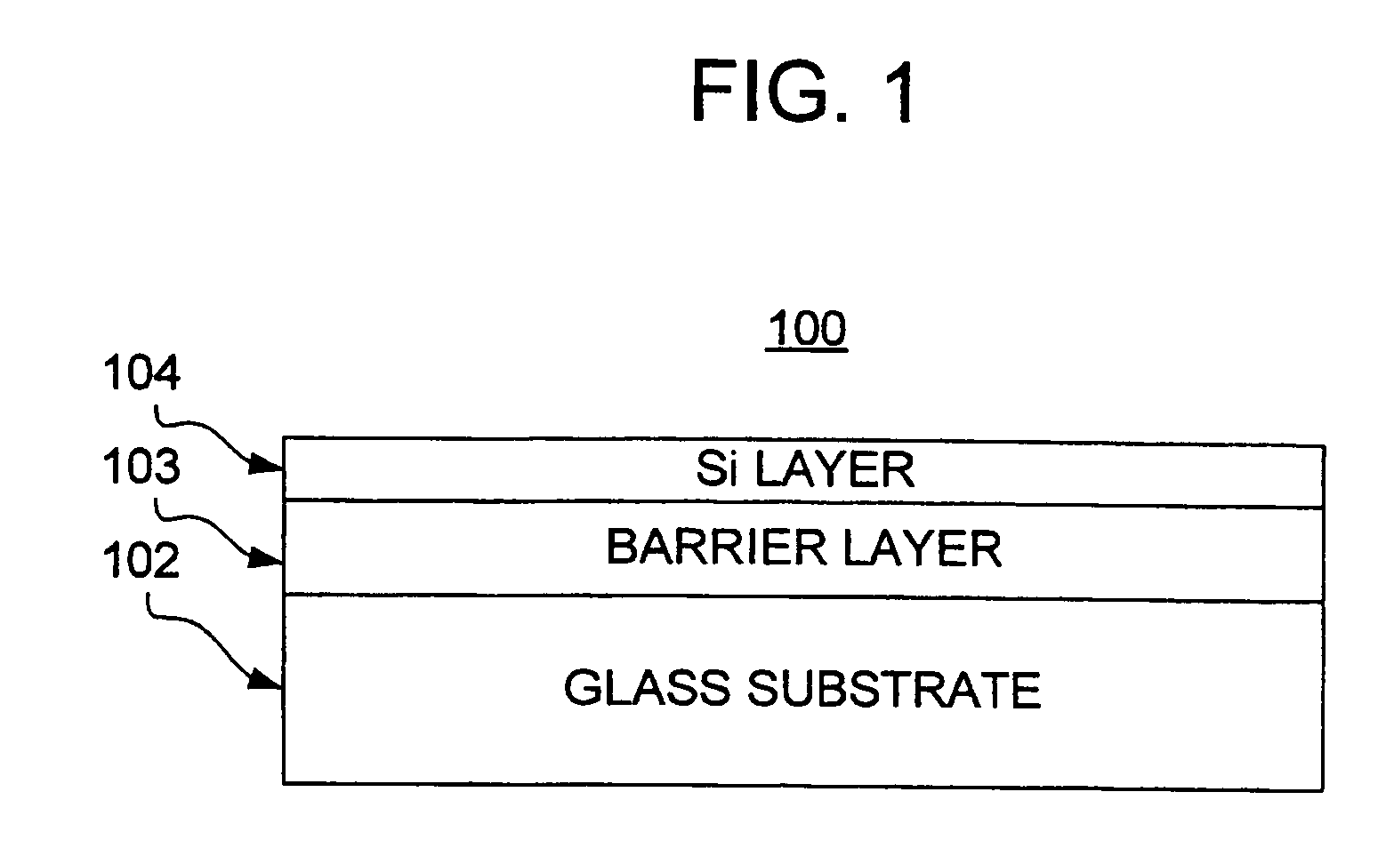
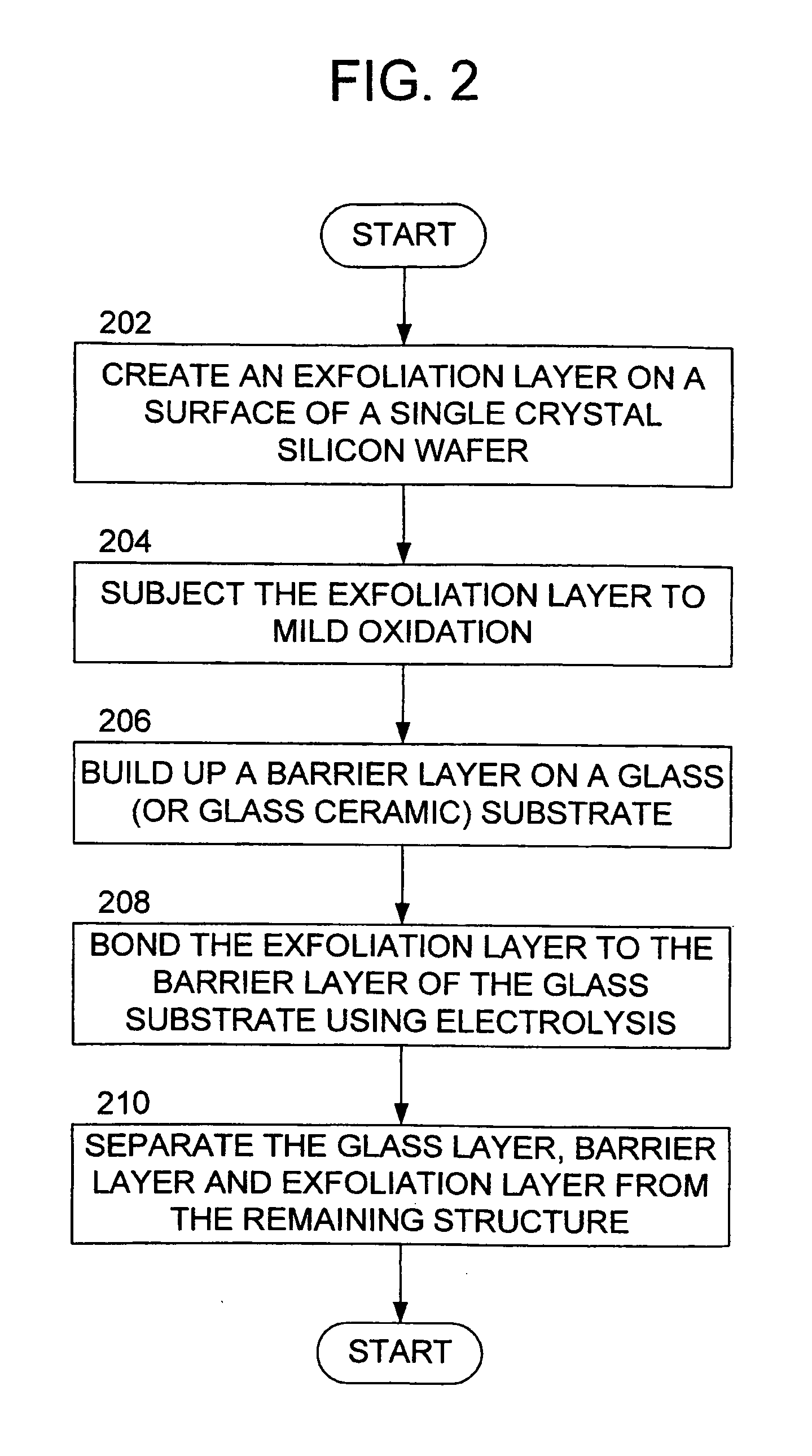
[0049] A silicon wafer of 100 mm diameter and 100 microns thick was hydrogen ion implanted at a dosage of 8×10¹⁶ ions / cm2 and an implantation energy of 100 KeV. The wafer was then treated in oxygen plasma to oxidize the surface groups. An EAGLE glass wafer of 100 mm diameter was then cleaned and coated with 200 nm of silica via a standard PECVD process to form a deposited barrier layer. The two wafers were then inserted into a Süss MicroTec SB6 bonder. The glass wafer was placed on the negative electrode and the silicon wafer was placed on the positive electrode and held away from the glass wafer with spacers. The two wafers were brought into contact and then heated to 525° C. (silicon wafer) and 575° C. (glass wafer) in a vacuum. A potential of 1750 Volts was applied across the wafer surface. The voltage was applied for 20 minutes, at the end of which the voltage was brought to zero and the wafers were cooled to room temperature. The wafers could be separated easily. An excellent qu
example 2
[0050] The experiment of Example 1 was repeated, except that the silica barrier layer thickness was increased to 500 nm. In this experiment, the silicon layer bond to the coated glass wafer was again successfully demonstrated via visual inspection and mechanical testing.
example 3
[0051] The experiment of Example 2 was repeated but in this case 100 nm of zirconium oxide was sputter coated onto the glass wafer to produce the barrier layer. The silicon layer bond was again successfully demonstrated via visual inspection and mechanical testing.
PUM
 Abstract
Description
Claims
Application Information
 - R&D Engineer
- R&D Manager
- IP Professional
- Industry Leading Data Capabilities
- Powerful AI technology
- Patent DNA Extraction
Browse by: Latest US Patents, China's latest patents, Technical Efficacy Thesaurus, Application Domain, Technology Topic.
© 2024 PatSnap. All rights reserved.Legal|Privacy policy|Modern Slavery Act Transparency Statement|Sitemap