Semiconductor memory device and method of production

a memory device and semiconductor technology, applied in the direction of semiconductor devices, basic electric elements, electrical equipment, etc., can solve the problem of limited pitch of the word line array and other problems

Inactive Publication Date: 2007-04-05
POLARIS INNOVATIONS
View PDF5 Cites 0 Cited by
  • Summary
  • Abstract
  • Description
  • Claims
  • Application Information

AI Technical Summary

Benefits of technology

This patented technology allows for more efficient use of space by allowing multiple terminal devices (such as sensors) within a single chip area to communicate wirelessly through signal lines without interference or crosstalking signals. It also includes methods like adding layers around certain parts of each device's circuitry to improve its performance. Overall, this innovation improves efficiency and reliability in wireless communication systems while reducing costs associated therewith

Problems solved by technology

This patented describes semiconducting memories used for storing data. These memories consists of multiple layers made up of small elements called bit-cells (BSC). To store more data on these memristive chips requires increasing their size due to increased demand placed upon them during manufacturing processes. However, this results in decreased space utilization within each chip layer.

Method used


Image

  • Semiconductor memory device and method of production
  • Semiconductor memory device and method of production
  • Semiconductor memory device and method of production

Examples


Embodiment Construction

[0044] The making and using of the presently preferred embodiments are discussed in detail below. It should be appreciated, however, that the present invention provides many applicable inventive concepts that can be embodied in a wide variety of specific contexts. The specific embodiments discussed are merely illustrative of specific ways to make and use the invention, and do not limit the scope of the invention.

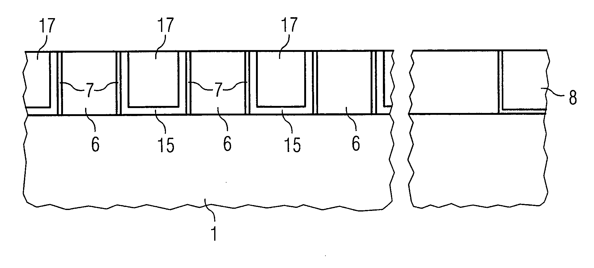
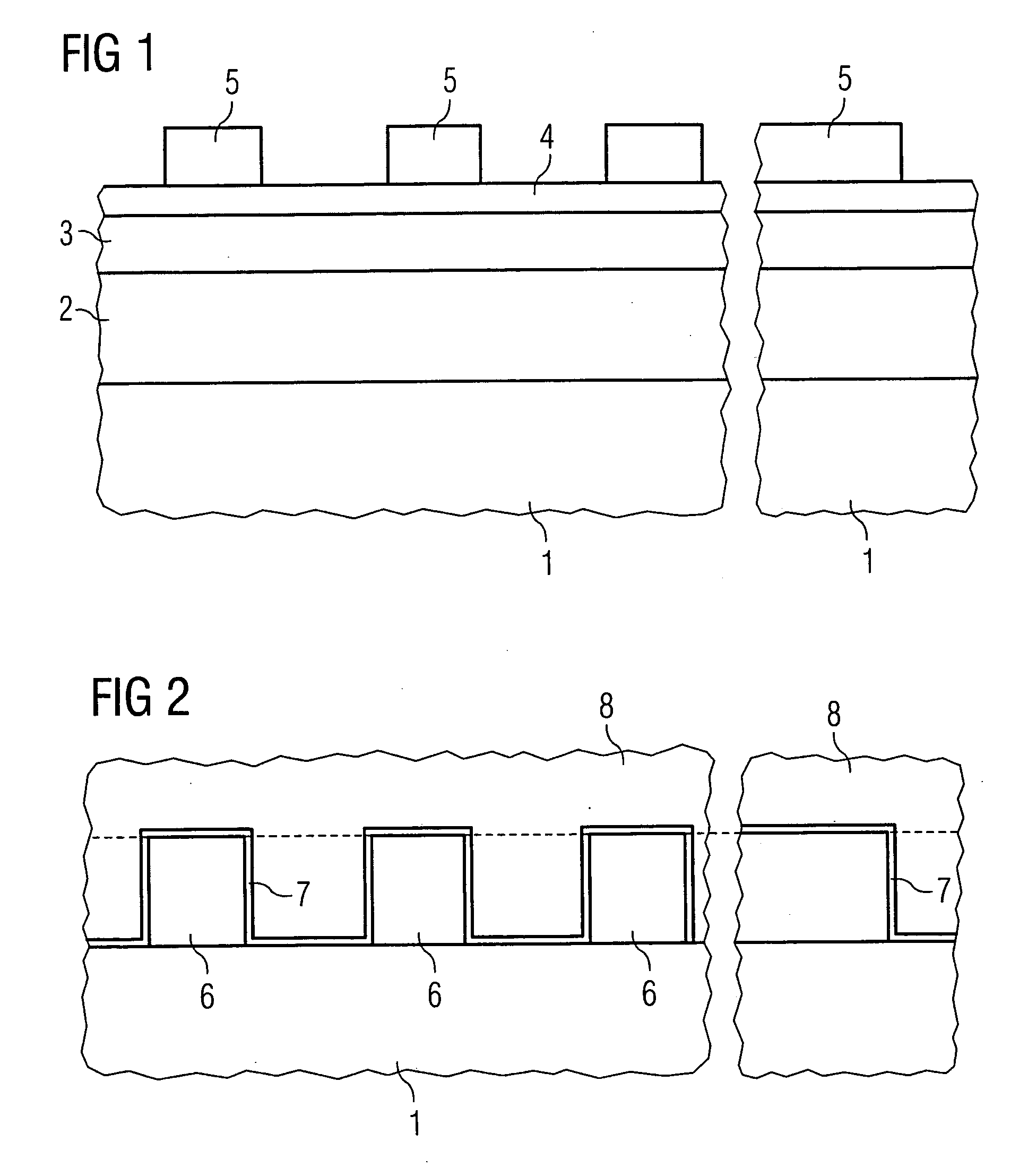
[0045] Preferred examples of the semiconductor memory device are described in conjunction with the figures with reference to the production steps of a preferred production method. The conductor tracks are provided as word lines in this example.

[0046]FIG. 1 shows a cross-section of a first intermediate product. A first word line layer 2 and a hard mask 3 are applied on a main surface of a semiconductor body 1, such as a substrate. The first word line layer 2 can be a layer sequence, typically formed of a first layer of doped polysilicon, followed by a second layer of metal or


PUM


Abstract

Final sections of the word lines are arranged in a staggered fashion to fan out and have larger lateral extensions than the word lines. Interspaces are filled with a dielectric material, and a mask is applied that partially covers the final sections and leaves contact areas in regions adjacent to the final sections and to the interspaces open. This mask is used to remove the dielectric material between the word line stacks. A second word line layer is applied and planarized to form second word lines between the first word lines, which have contact areas arranged in a staggered fashion to fan out like the final sections of the first word lines.

Description


Claims


Application Information

Patent Timeline
Owner POLARIS INNOVATIONS
Why Eureka
Try Eureka