Methods for uniform metal impregnation into a nanoporous material
- Summary
- Abstract
- Description
- Claims
- Application Information
AI Technical Summary
Problems solved by technology
Method used
Image

Examples
Example
Example 1
Construction of a Porous Silicon Substrate
Formation of Porous Nanocrystalline Silicon
[0058] Methods for making nanocrystalline porous silicon 110, 210 are known in the art (e.g., U.S. Pat. No. 6,017,773). A layer of nanocrystalline porous silicon 110, 210 may be formed electrochemically as disclosed in Petrova-Koch et al. (Appl. Phys. Let. 61:943,1992). Depending on the particular application, the silicon may be lightly or heavily p-doped or n-doped prior to etching to regulate the characteristics of the porous silicon substrate 110, 210. Single crystal silicon ingots may be grown by the well known Czochralski method (e.g., http: / / www.msil.ab.psiweb.com / english / msilhist4-e.html). A single crystal silicon wafer may be treated with anodic etching in dilute HF / electrolyte to form a nanocrystalline porous silicon substrate 110, 210. Alternatively, chemical etching in a solution of HF, nitric acid and water may be used without anodic etching. Ethanol may be used as a
Example
Example 2
Metal Coating of Porous Silicon by Thermal Decomposition
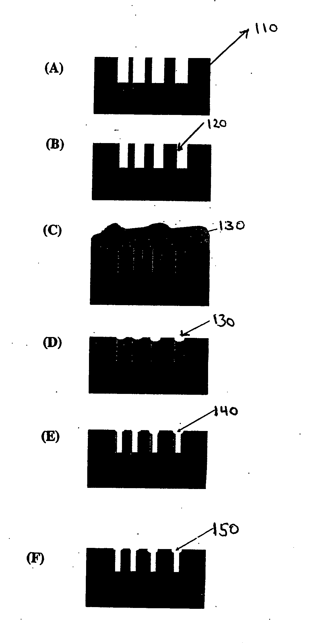
[0062]FIG. 1 illustrates an exemplary method for uniformly impregnating metal 150 into nanoporous silicon 110. The surface of the porous silicon 110 is oxidized to silicon dioxide 120 (FIG. 1B). A metal salt solution 130 is diffused into the porous matrix 110 (FIG. 1C) and dried (FIG. 1E). The dried metal salt 140 is thermally decomposed inside the pores to form a uniform metal layer 150 (FIG. 1F). Oxidation of the porous silicon surface 110 enables complete wetting of porous silicon 110 in the metal salt solution 130, while preventing spontaneous immersion coating, which causes pore blockage. The dry metal salt 140 is thermally decomposed in a furnace and pure metal 150 is deposited on the side walls of the nanopores. A uniform, thin metal 150 coating of nanoporous silicon 110 may be obtained without plugging the pores, as often observed with standard methods of metal 150 infiltration into nanoporous silicon 110. Curr
Example
Example 3
Raman Detection of Analytes
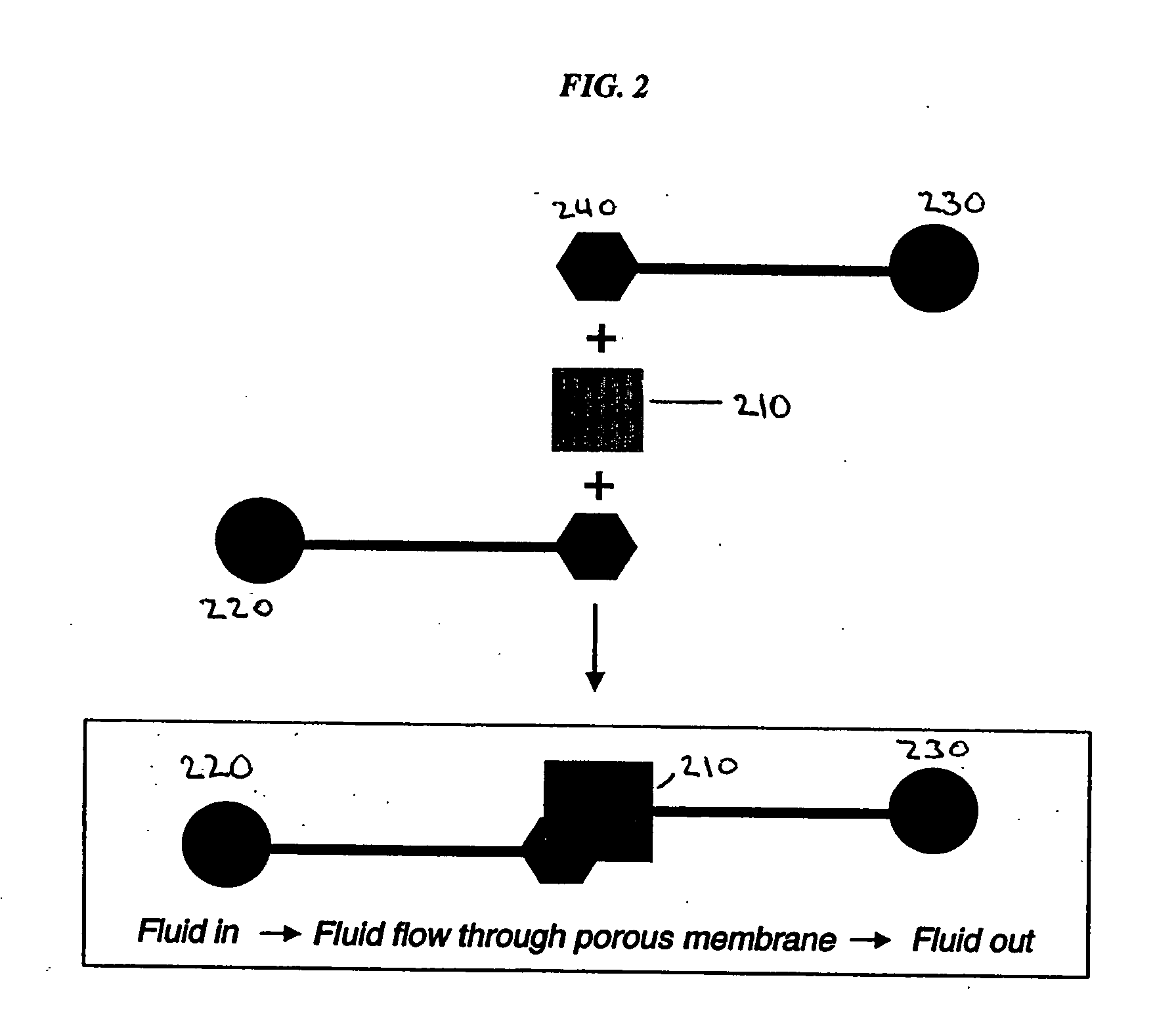
[0068] A Raman active metal-coated substrate 110, 210 formed as disclosed above may be incorporated into a system 400 for Raman detection, identification and / or quantification of analytes, as exemplified in FIG. 4. The substrate 110, 210 may be incorporated into, for example, a flow through cell, connected via inlet and outlet channels to one or more solvent reservoirs 220 and a waste reservoir 230. Alternatively, the inlet channel may be connected to one or more other devices, such as a sample injector and / or reaction chamber. Analytes may enter the flow through cell and pass across the Raman active substrate 110, 210, where they may be detected by a Raman detection unit. The detection unit may comprise a Raman detector 420 and a light source 410, such as a laser. The laser 410 may emit an excitation beam, activating the analytes and resulting in emission of Raman signals. The Raman signals are detected by the detector 420. In certain embodim
PUM
| Property | Measurement | Unit |
|---|---|---|
| Depth | aaaaa | aaaaa |
Abstract
Description
Claims
Application Information
 - R&D Engineer
- R&D Manager
- IP Professional
- Industry Leading Data Capabilities
- Powerful AI technology
- Patent DNA Extraction
Browse by: Latest US Patents, China's latest patents, Technical Efficacy Thesaurus, Application Domain, Technology Topic.
© 2024 PatSnap. All rights reserved.Legal|Privacy policy|Modern Slavery Act Transparency Statement|Sitemap