Optical fiber impulse sensor fabricating method

a technology of optical fiber and impulse sensor, which is applied in the direction of instruments, other domestic objects, optical elements, etc., can solve the problems of time-consuming insertion of hpof into the cavity and poor workability, and achieve the effect of improving workability

Inactive Publication Date: 2007-08-09
HITACHI CABLE +1
View PDF1 Cites 5 Cited by
  • Summary
  • Abstract
  • Description
  • Claims
  • Application Information

AI Technical Summary

Benefits of technology

This technology can make things easier by improving their ability to perform better than previous versions or even making them more efficient at performing certain tasks.

Problems solved by technology

The technical problem addressed in this patented technology relates to improving the efficiency at manufacturing optics fibers used in impact sensors due to difficulties associated with handling these materials during production processes.

Method used


Image

  • Optical fiber impulse sensor fabricating method
  • Optical fiber impulse sensor fabricating method
  • Optical fiber impulse sensor fabricating method

Examples


Embodiment Construction

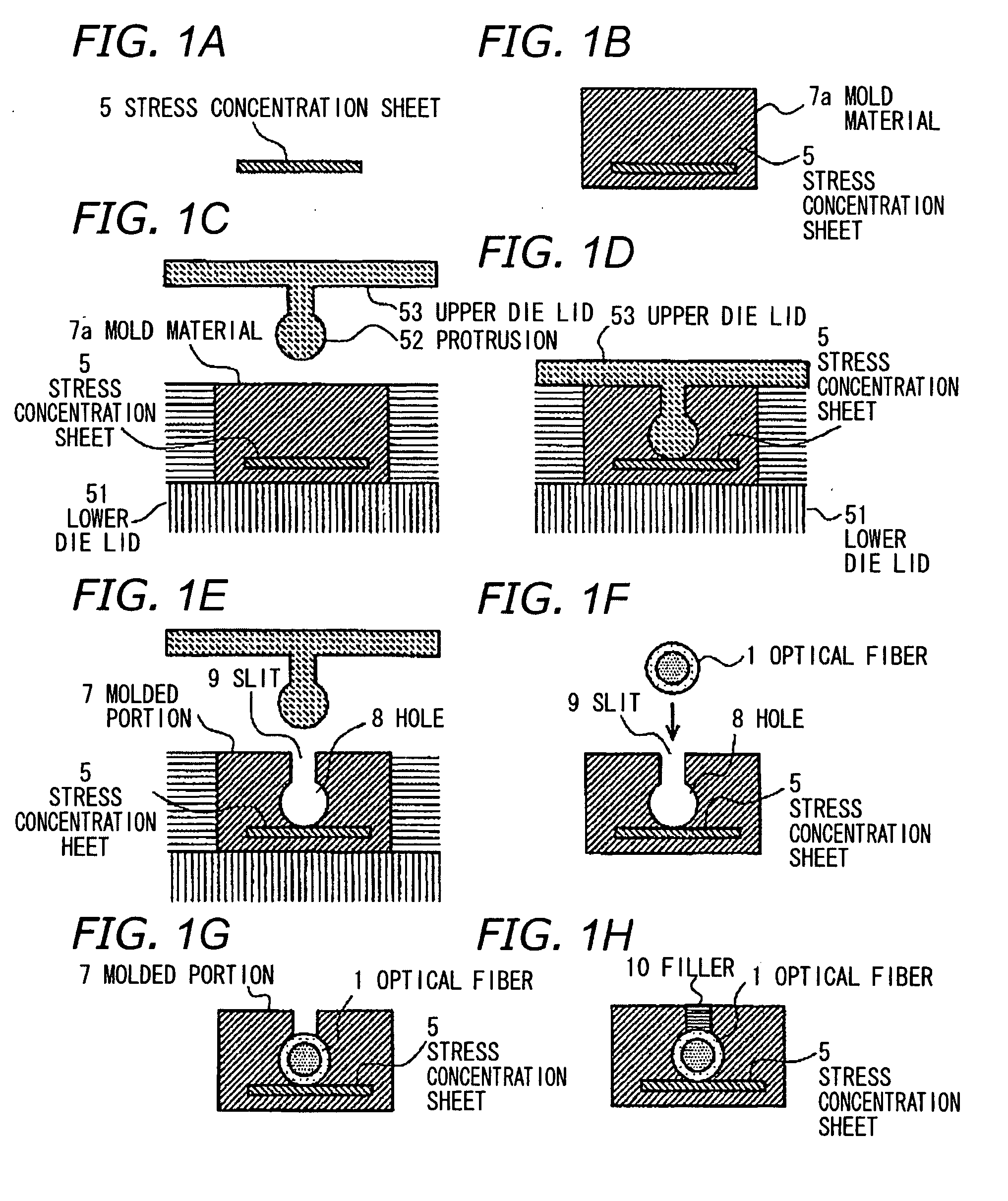
Optical Fiber Impulse Sensor Fabrication Method FIGS. 1A-1H show a process for fabricating an optical fiber impulse sensor according to the present invention.

[0027] Around the perimeter of a stress concentration sheet 5 shown in FIG. 1A, is extruded and molded a mold material 7a, as shown in FIG. 1B. It should be noted, however, that this invention is applicable even in the case of no stress concentration sheet 5.

[0028] As shown in FIG. 1C, this is followed by mounting the mold material 7a to a lower die lid 51 for pressing and molding. An upper die lid 53 for pressing and molding, which has a protrusion 52 formed in an integral shape of an optical fiber insertion hole 8 and an insertion slit 9 (in the figure, a shape having a substantially keyhole-shaped cross section) is caused to face the lower die lid 51 for pressing and molding.

[0029] As shown in FIG. 1D, the upper die lid 53 is pressed down and fitted on the lower die lid 51, and as shown in FIG. 1E, is then removed upward th


PUM


Abstract

A method for fabricating an optical fiber impulse sensor having an optical fiber and a molded portion molded around the perimeter of the optical fiber. The method forms, in the molded portion, an optical fiber insertion hole and an optical fiber insertion slit for inserting the optical fiber into the optical fiber insertion hole. The method inserts the optical fiber from the slit into the optical fiber insertion hole.

Description


Claims


Application Information

Patent Timeline
Owner HITACHI CABLE
Why Eureka
Try Eureka