Semiconductor memory device
- Summary
- Abstract
- Description
- Claims
- Application Information
AI Technical Summary
Benefits of technology
Problems solved by technology
Method used
Image

Examples
first embodiment
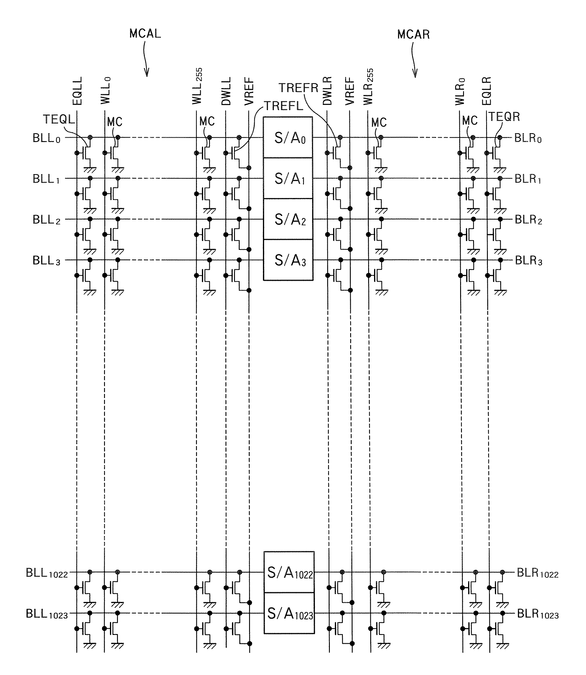
[0041]FIG. 1 is a circuit diagram of the configuration of an FBC memory device according to a first embodiment of the present invention. The FBC memory device includes memory cells MC, sense amplifiers S / Ai (where i is an integer) (hereinafter, also “S / A”), word lines WLLi and WLRi (hereinafter, also “WL”), bit lines BLLi and BLRi (hereinafter, also “BL”), equalizing lines EQLL and EQLR (hereinafter, also “EQL”), equalizing transistors TEQL and TEQR (hereinafter, also “TEQ”), reference potential lines VREF, reference transistors TREFL and TREFR (hereinafter, also “TREF”), and dummy word lines DWLL and DWLR (hereinafter, also “DWL”). It is to be noted that “reference potential” refers to a voltage with which data “1” or “0” is compared when the data “1” or “0” is detected.
[0042]The memory cells MC are arranged in a matrix and memory cell arrays MCAL and MCAR (hereinafter, also “MCA”) are constituted by the memory cells MC. The word lines WL extend in a row direction and are connecte
second embodiment
[0079]FIG. 8 is a circuit diagram of a sense amplifier S / A according to a second embodiment of the present invention. The sense amplifier S / A according to the second embodiment differs from that according to the first embodiment in that the sense amplifier S / A includes a first flip-flop FF11 constituted by PMOS transistors TP10 and TP11 and a second flip-flop FF12 constituted by PMOS transistors TP12 and TP13 instead of the flip-flops FF1. The other configurations of the sense amplifier S / A according to the second embodiment can be the same as those according to the first embodiment.
[0080]The transistors TP10 and TP11 are connected in series between the sense nodes SNL and SNR. The transistors TP12 and TP13 are connected in series between the sense nodes SNL and SNR. Gates of the transistors TP10 and TP12 are connected in common to the sense node SNR. Gates of the transistors TP11 and TP13 are connected in common to the sense node SNL. Namely, the gates of the transistors TP10
third embodiment
[0088]FIG. 10 is a circuit diagram of a sense amplifier S / A according to a third embodiment of the present invention. The sense amplifier S / A according to the third embodiment differs from that according to the second embodiment in that the sense amplifier S / A according to the third embodiment includes a PMOS transistor TP30 serving as a first short-circuiting switch and a PMOS transistor TP31 serving as a second short-circuiting switch in place of the PMOS transistor TP3 shown in FIG. 8. The other configurations of the sense amplifier S / A according to the third embodiment can be the same as those according to the second embodiment. The sum of sizes (W / L) of the transistors TP30 and TP31 can be set almost equal to the size (W / L) of the transistor TP3 according to the first and the second embodiments. The size (W / L) of the transistor TP30 needs to be sufficiently large to quickly equalize the paired sense nodes during precharging (before to and after t8). However, the size
PUM
 Abstract
Description
Claims
Application Information
 - R&D Engineer
- R&D Manager
- IP Professional
- Industry Leading Data Capabilities
- Powerful AI technology
- Patent DNA Extraction
Browse by: Latest US Patents, China's latest patents, Technical Efficacy Thesaurus, Application Domain, Technology Topic.
© 2024 PatSnap. All rights reserved.Legal|Privacy policy|Modern Slavery Act Transparency Statement|Sitemap