Electrostatic discharge protection apparatus and method therefor

Active Publication Date: 2009-05-07
NXP USA INC
View PDF10 Cites 5 Cited by
  • Summary
  • Abstract
  • Description
  • Claims
  • Application Information

AI Technical Summary

Problems solved by technology

However, an interconnecting node between the first and second NPN bipolar transistors “floats”, i.e. does not remain at a constant potential, and so when an Electromagnetic Interference or a fast transient event occurs, parasitic elements, for example parasitic capacitances of the fir

Method used


Image

  • Electrostatic discharge protection apparatus and method therefor
  • Electrostatic discharge protection apparatus and method therefor
  • Electrostatic discharge protection apparatus and method therefor

Examples


Embodiment Construction

[0009]Throughout the following description identical reference numerals will be used to identify like parts.

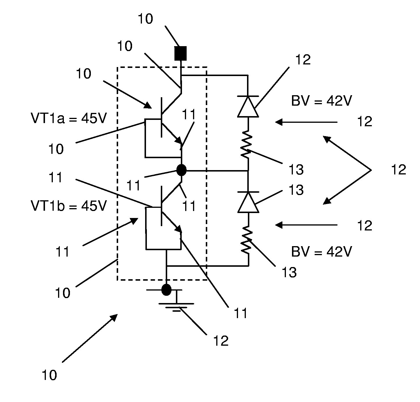
[0010]Referring to FIG. 1, an Electrostatic Discharge (ESD) protection apparatus 100 comprises a stack 101 having a first NPN bipolar transistor 102 having a first collector terminal 104 thereof coupled to a pad 106 of an integrated circuit (not shown) in order to protect circuitry or a device (also not shown) coupled to the pad 106. The first NPN transistor 102 is self-biased and so has a first base terminal 108 coupled to a first emitter terminal 110 thereof.

[0011]The first base and first emitter terminals 108, 110 of the first NPN transistor 102 are coupled to a second collector terminal 112 of a second NPN bipolar transistor 114. As a result of the coupling of the first NPN transistor 102 to the second NPN transistor 114, a notional topological node 115 exists between the first and second NPN transistors 102, 114.

[0012]The second NPN transistor 114 is also self-biased and so


PUM


Abstract

An electrostatic discharge protection apparatus comprises a stack arrangement having a first electrostatic discharge protection element and a second electrostatic discharge protection element. The stack arrangement is arranged to provide a bias potential between the first and second electrostatic discharge protection elements. In one embodiment, the bias potential can be achieved by a clamp arrangement coupled across the stack arrangement.

Description


Claims


Application Information

Patent Timeline
Owner NXP USA INC
Why Eureka
Try Eureka