Semiconductor device for electrostatic discharge protection
a semiconductor and electrostatic discharge technology, applied in the direction of transistors, diodes, electric devices, etc., can solve the problems of damage to the ic, many conventional esd clamps suffer from being too slow to trigger, so as to speed up the triggering of scr, and accelerate the triggering
- Summary
- Abstract
- Description
- Claims
- Application Information
AI Technical Summary
Benefits of technology
Problems solved by technology
Method used
Image

Examples
Embodiment Construction
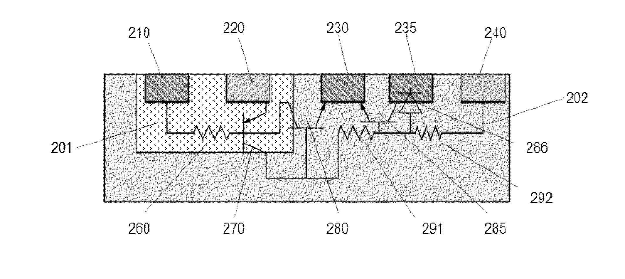
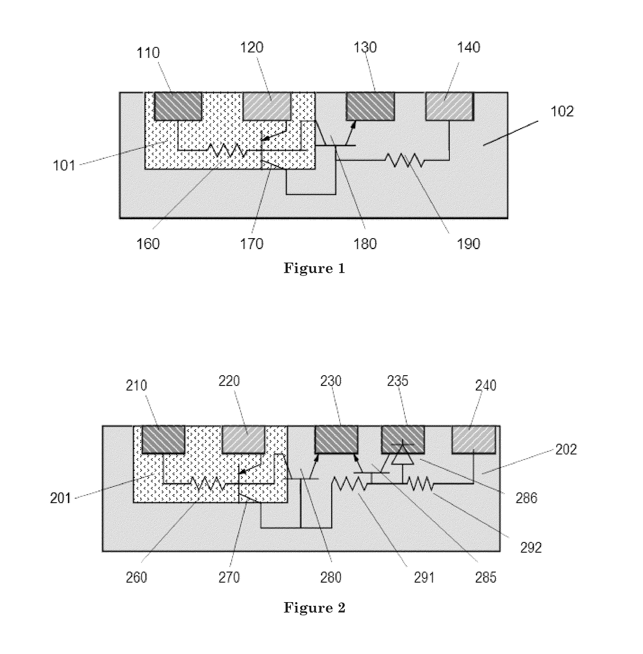
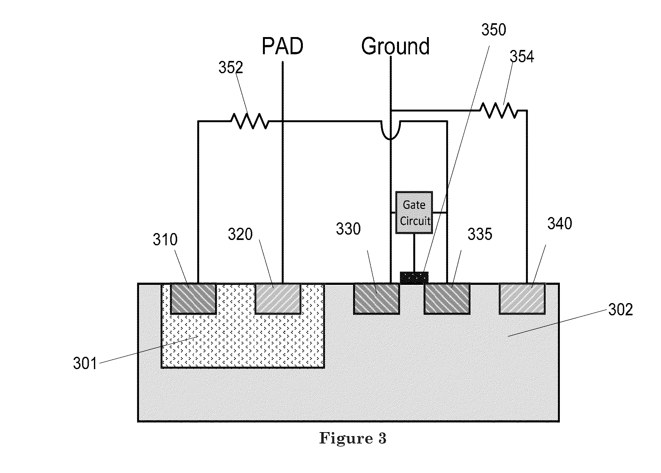
[0056]The circuits described herein comprise wells of a conductivity type, wherein the conductivity type may be either N-type or P-type. In the following embodiments, a circuit may be implemented with conductivity types as depicted in the accompanying figure. Alternatively, the embodiments may be implemented such that each conductivity type is the opposite of that shown in the figures and described in the accompanying text. For instance, wherein a PNP bipolar transistor is described comprising a first region of P conductivity type, a second region of N conductivity type, and a third region of P conductivity type, the conductivities of the regions may be flipped such that an NPN bipolar transistor may be alternatively implemented comprising the first region of N conductivity type, the second region of P conductivity type, and the third region of N conductivity type.
[0057]In the following descriptions, common numerical designations may be used for similar, corresponding parts across mult
PUM
 Abstract
Description
Claims
Application Information
 - R&D Engineer
- R&D Manager
- IP Professional
- Industry Leading Data Capabilities
- Powerful AI technology
- Patent DNA Extraction
Browse by: Latest US Patents, China's latest patents, Technical Efficacy Thesaurus, Application Domain, Technology Topic.
© 2024 PatSnap. All rights reserved.Legal|Privacy policy|Modern Slavery Act Transparency Statement|Sitemap