Phase lock oscillator and wireless communications device including phase lock oscillator
a phase lock and wireless communication technology, applied in the direction of pulse manipulation, pulse technique, electrial characteristics varying frequency control, etc., can solve the problems of affecting the actual device on which the pll is mounted, the noise of external circuits, and the change of voltage of the power sour
- Summary
- Abstract
- Description
- Claims
- Application Information
AI Technical Summary
Benefits of technology
Problems solved by technology
Method used
Image

Examples
first embodiment
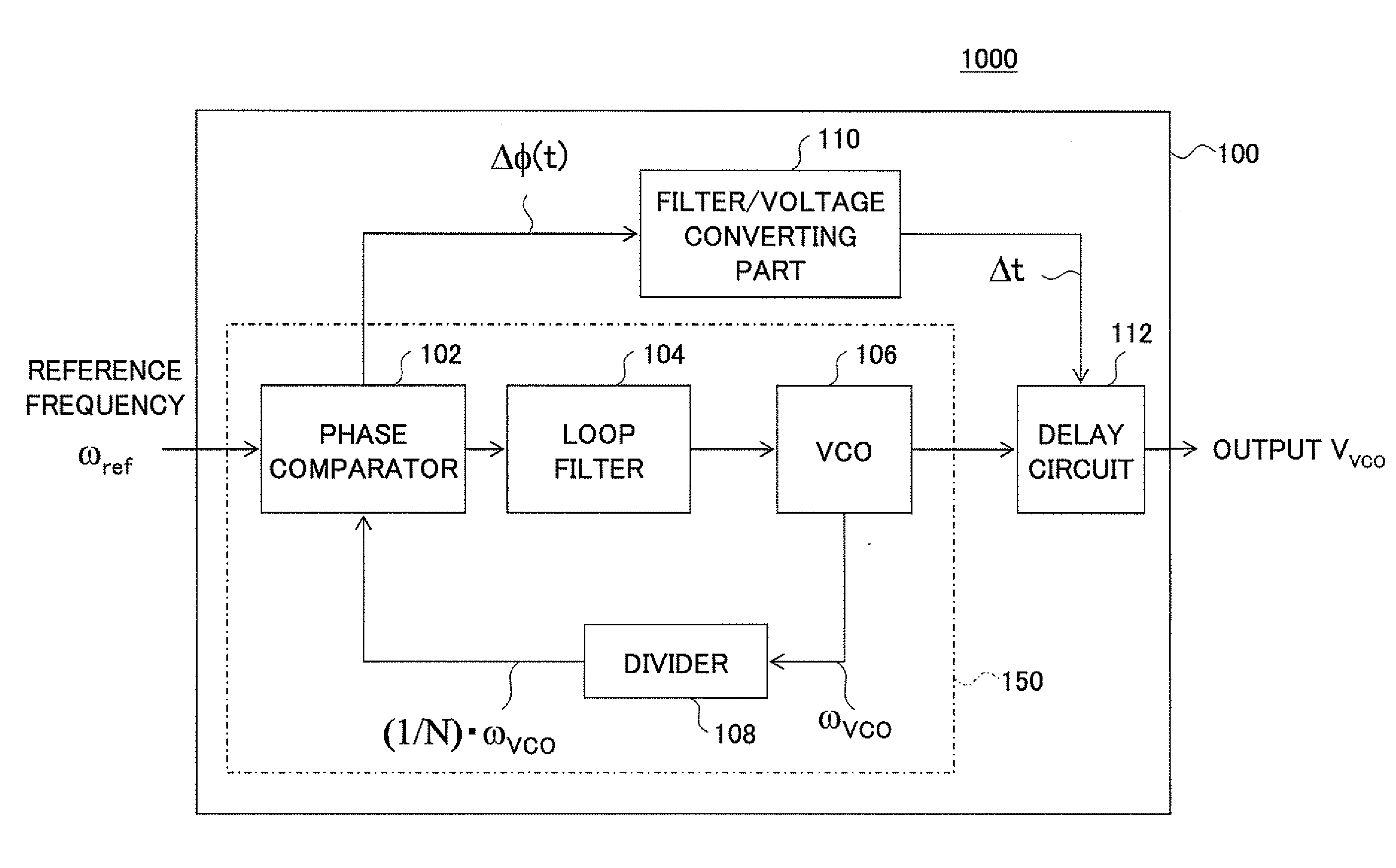
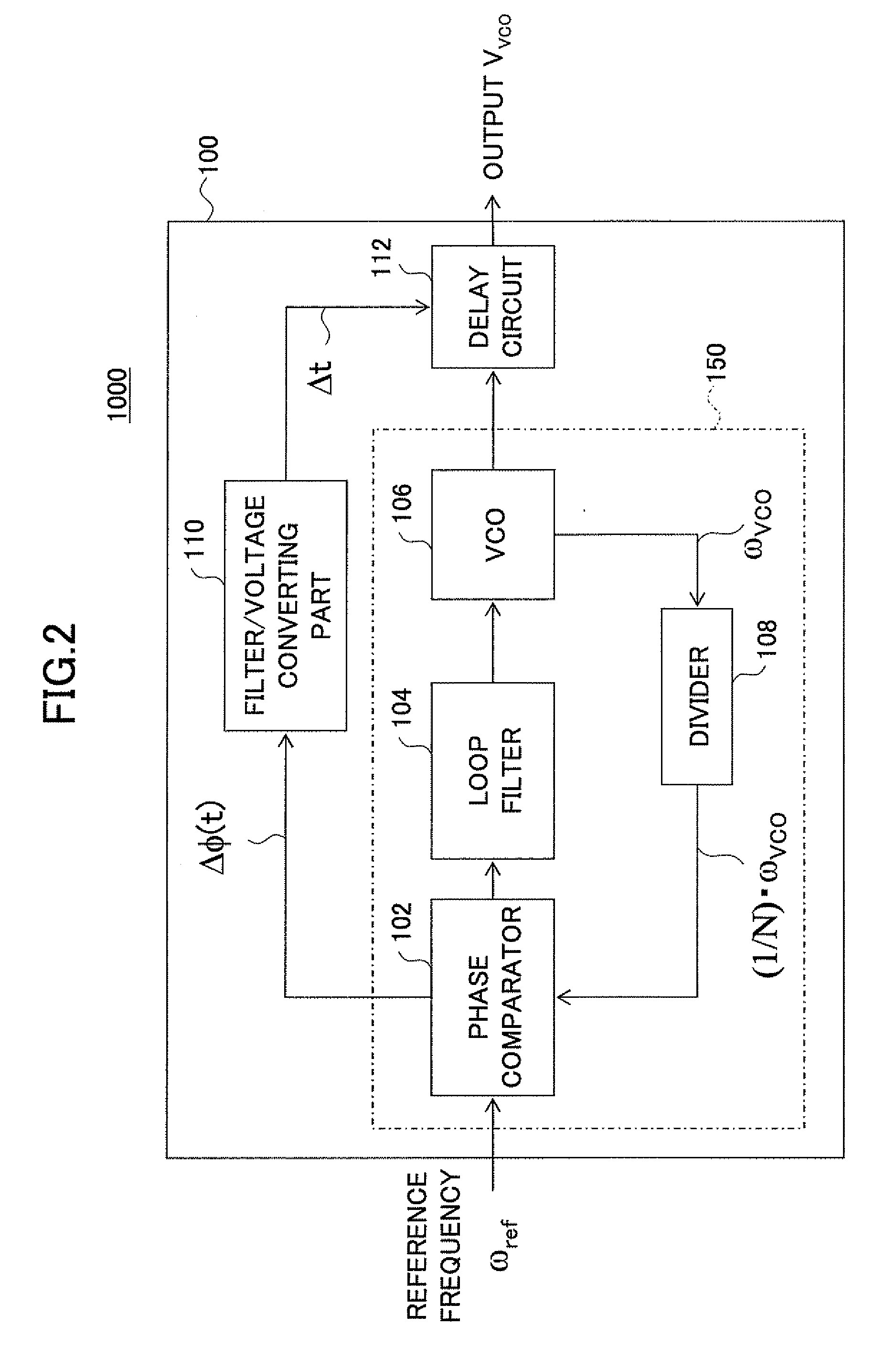
[0032]First, a phase lock oscillator (may also be referred to as “local oscillator” or “frequency synthesizer”) 100 according to the first embodiment of the present invention is described with reference to FIG. 2.
[0033]In this embodiment, the phase lock oscillator 100 is mounted on, for example, a wireless communications device 1000. That is, the wireless communication device 1000 includes the phase lock oscillator 100.
[0034]The phase lock oscillator 100 includes a phase comparator 102. A signal output from a VCO 106 and divided by a divider 108 and a reference signal of a reference frequency fref (reference angular frequency ωref) are input to the phase comparator 102. The reference signal is generated by an oscillator (e.g., crystal oscillator). The phase comparator 2 compares a phase of the signal output from the VCO 106 and divided by the divider 108 and a phase of the reference signal. In a case where the phases are different, the phase comparator 102 generates a voltage and a cur
second embodiment
[0068]Next, a phase lock oscillator 100A according to a second embodiment of the present invention is described with reference to FIG. 15.
[0069]The phase lock oscillator 100A has substantially the same configuration as the above-described phase lock oscillator 100 of the first embodiment except that another delay circuit (delaying part) 116 is provided in the phase lock oscillator 100A. A signal output from the VCO 106 is input to the delay circuit 116. The delay circuit 116 outputs a signal to the delay circuit 112.
[0070]In the phase lock oscillator 100 of the first embodiment, the output of the VCO 106 is input to the delay circuit 112 via the divider 108, the phase comparator 102, and the loop filter 104. With this configuration, phase correction performed by a series of processes is delayed one cycle or more from the instant phase offset that occurs in the output of the VCO 106. Therefore, error may occur in a case where phase changes at an interval faster than a reference frequenc
third embodiment
[0072]Next, a phase lock oscillator 100B according to a third embodiment of the present invention is described with reference to FIG. 16.
[0073]The phase lock oscillator 100B has substantially the same configuration as the phase lock oscillator 100 of the first embodiment except that a VCO 118 configured as a DLL (Delay Locked Loop) is provided in the phase lock oscillator 100B.
[0074]With the VCO 118 having the DLL configuration, an oscillation frequency can be selected by controlling a switching time with a bias voltage from an array of inverters forming a delay loop. The same as the PLL, frequency control is performed by controlling the delay amount of the delay loop according to a result of phase comparison by the phase comparator 102. Accordingly, instantaneous phase correction is performed by the delay circuit 112 provided outside the delayed loop of the VCO 118. With the VCO 118 being configured as a DLL, the result of phase comparison is used for frequency control by modifying th
PUM
 Abstract
Description
Claims
Application Information
 - R&D Engineer
- R&D Manager
- IP Professional
- Industry Leading Data Capabilities
- Powerful AI technology
- Patent DNA Extraction
Browse by: Latest US Patents, China's latest patents, Technical Efficacy Thesaurus, Application Domain, Technology Topic.
© 2024 PatSnap. All rights reserved.Legal|Privacy policy|Modern Slavery Act Transparency Statement|Sitemap