Etching method for forming a multi-step surface on a substrate
a multi-step surface and substrate technology, applied in the field of etching methods using photoresist, can solve the problems of affecting the quality of photoresist, increasing the overall cost, and complication of the manufacture process flow, so as to reduce the production cost, simplify the manufacturing process, and reduce the alignment problem and lead time
- Summary
- Abstract
- Description
- Claims
- Application Information
AI Technical Summary
Benefits of technology
Problems solved by technology
Method used
Image

Examples
Embodiment Construction
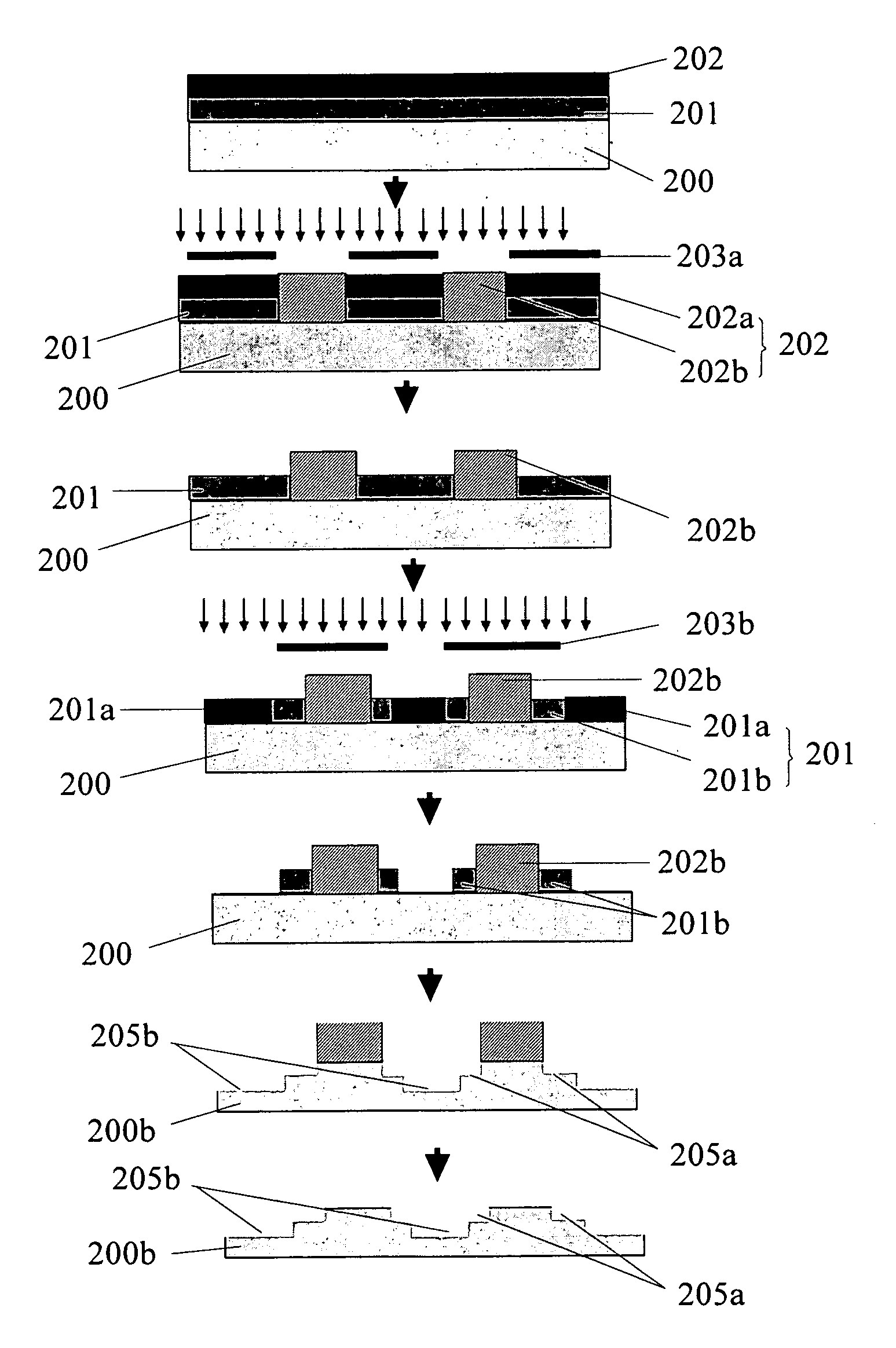
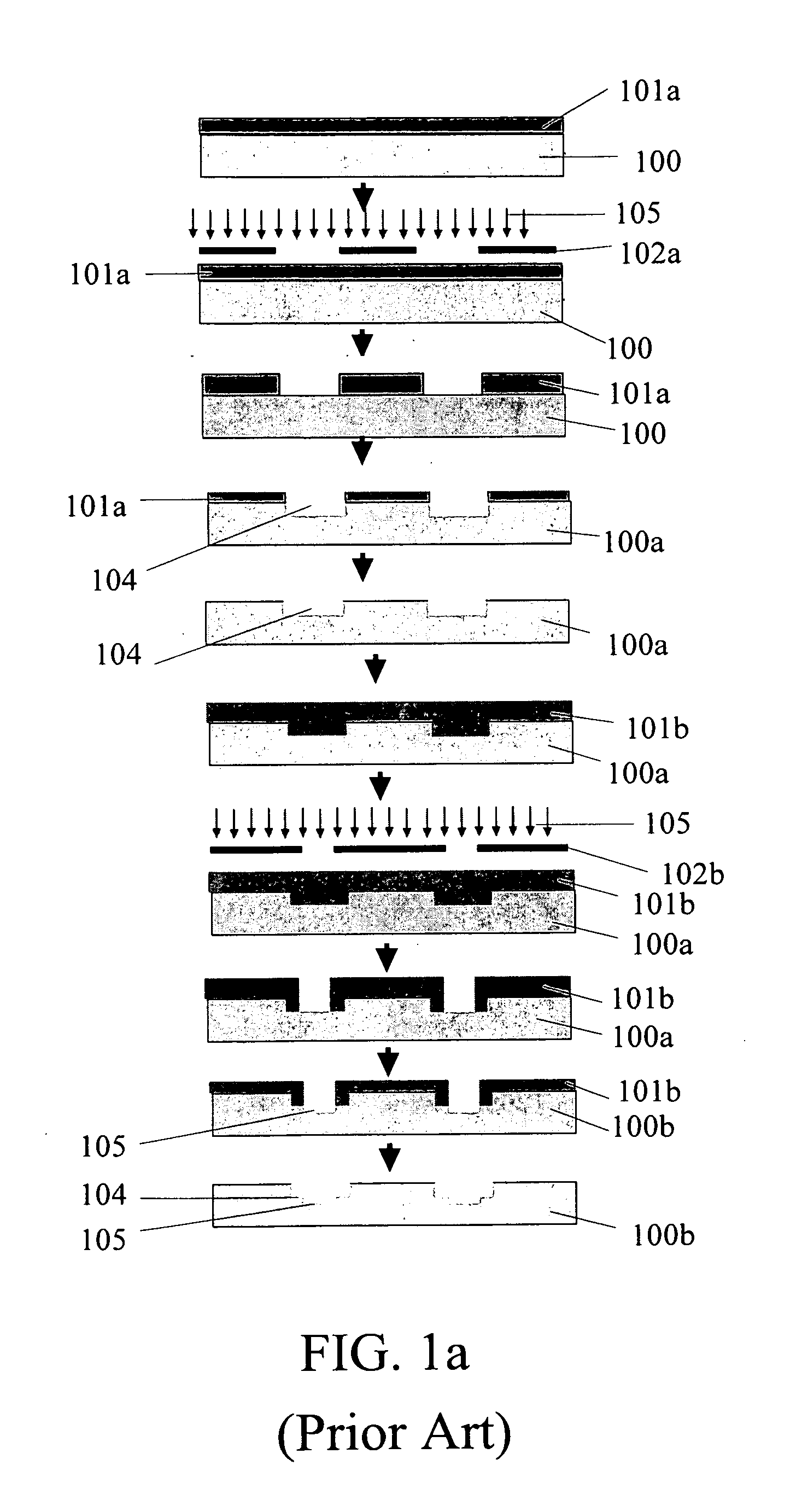
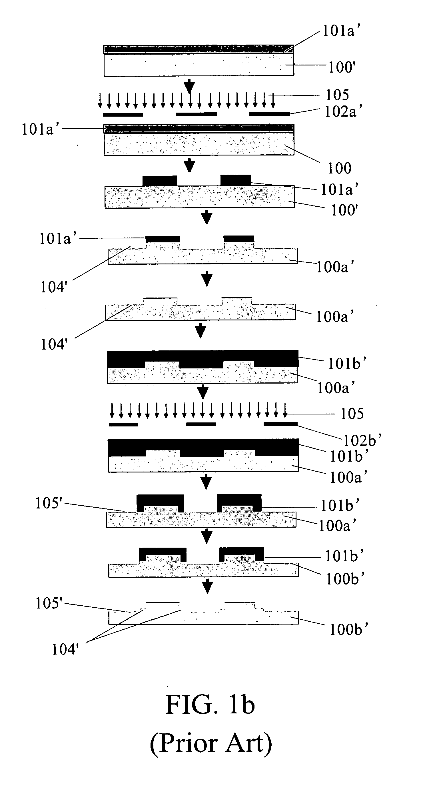
[0040]Various preferred embodiments of the invention will now be described with reference to the figures, wherein like reference numerals designate similar parts throughout the various views. As indicated above, the invention is directed to an etching method for forming a multi-step surface on a substrate, which is capable of simplifying the manufacturing process and reducing the cost.
[0041]Referring to FIG. 2, the deeper layer represents a negative photo-resist, while the shallower one represents a positive photo-resist. Taken two layers of photo-resists as an example, a preferred embodiment of the etching method according to the present invention is described in detail as followed.
[0042]Firstly, provide a substrate 200, which can be a wafer to be etched, a semiconductor substrate, or an incomplete semiconductor device. Then coat a first photo-resist layer 201 formed by positive photo-resist on a predetermined surface of the substrate 200 and bake the first photo-resist layer 201 to p
PUM
 Abstract
Description
Claims
Application Information
 - R&D Engineer
- R&D Manager
- IP Professional
- Industry Leading Data Capabilities
- Powerful AI technology
- Patent DNA Extraction
Browse by: Latest US Patents, China's latest patents, Technical Efficacy Thesaurus, Application Domain, Technology Topic.
© 2024 PatSnap. All rights reserved.Legal|Privacy policy|Modern Slavery Act Transparency Statement|Sitemap