Process for production of gallium nitride-based compound semiconductor light emitting device
a gallium nitride and light-emitting device technology, which is applied in the manufacture of semiconductor/solid-state devices, semiconductor devices, electrical equipment, etc., can solve the problems of inability to achieve high light emission intensity, side effects of requiring a higher driving voltage, and the relationship between this ratio and the driving voltage of the light-emitting device has not been determined. achieve the effect of low driving voltage and high light emission intensity
- Summary
- Abstract
- Description
- Claims
- Application Information
AI Technical Summary
Benefits of technology
Problems solved by technology
Method used
Image

Examples
example 1
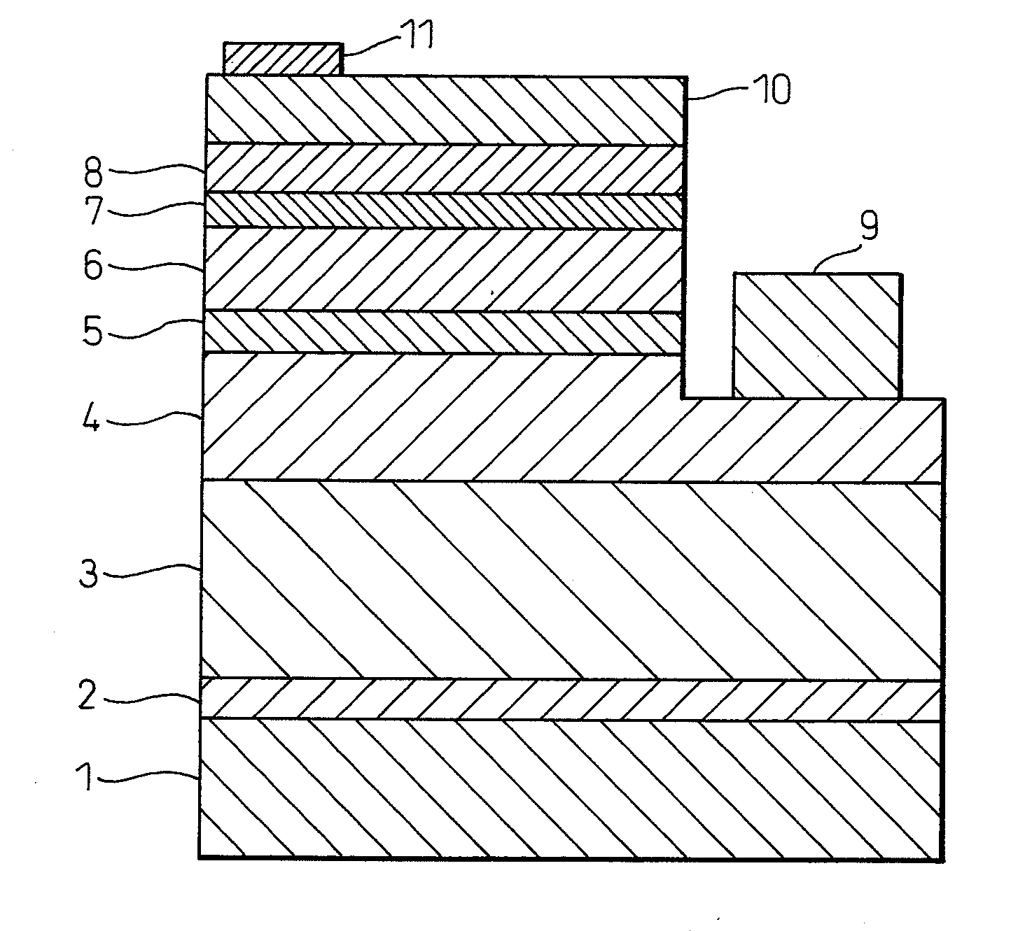
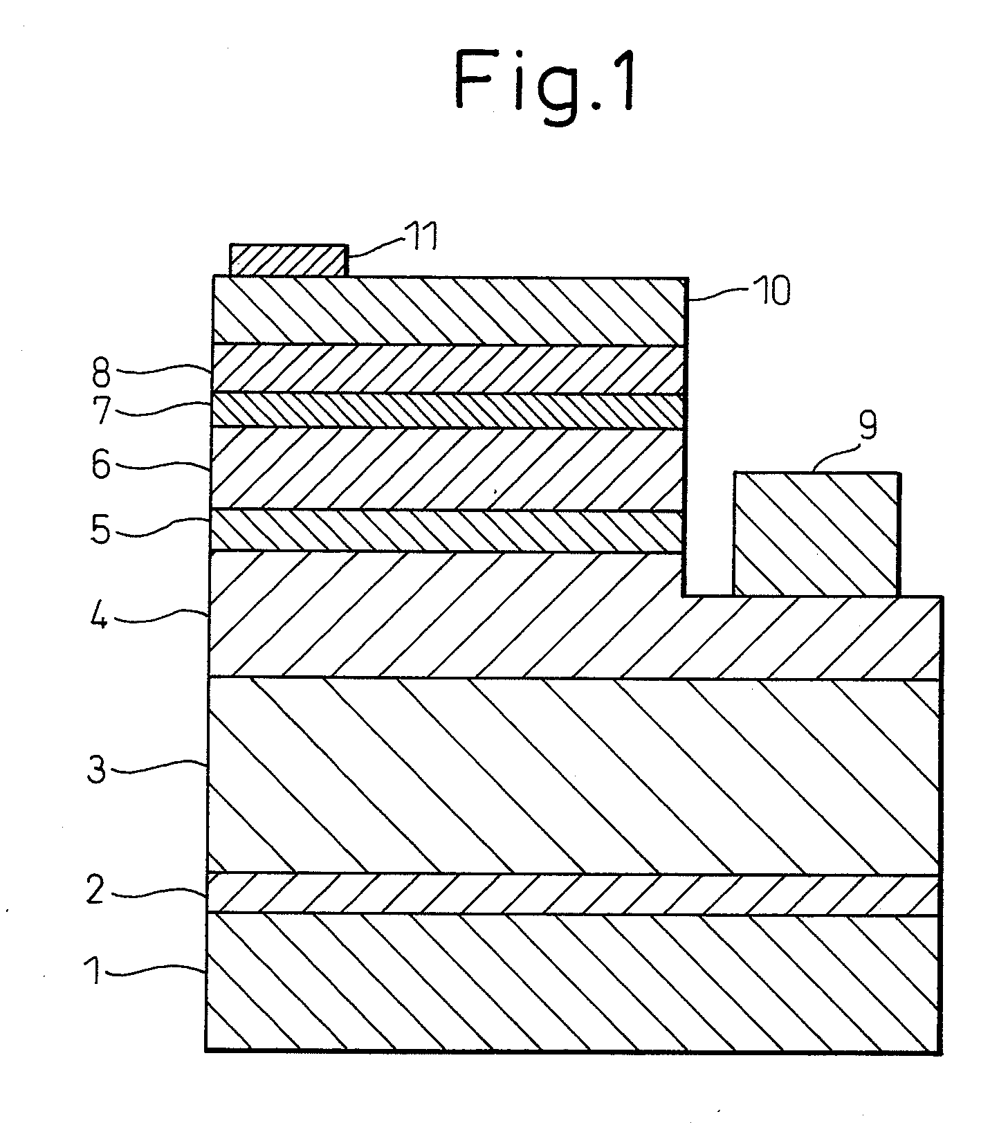
[0074]A sapphire substrate was set on a susceptor, and TMAl and NH3 were supplied together with H2 carrier gas onto the substrate while controlling the pressure to 20 kPa (200 mbar) and the temperature to 1100° C., to form an AlN buffer layer. The growth time was 10 minutes.
[0075]Next, TMGa and NH3 were supplied with a pressure of 40 kPa (400 mbar) and a temperature of 1030° C. for 3-hour growth of an undoped GaN underlying layer on the AlN buffer layer. SiH4 was then supplied as an n-type dopant while maintaining the same pressure and temperature, for 1-hour growth of an n-type GaN layer. This procedure formed an n-type contact layer.
[0076]Next, the carrier gas was switched from H2 to N2 with a pressure of 40 kPa (400 mbar) and a temperature of 750° C., and TEGa and TMIn were supplied for 90-minute growth of an n-type GaxIn1-xN layer. SiH4 was simultaneously supplied as the dopant. The TMIn supply rate was adjusted for an In composition of 1−X=0.02. This procedure formed an n-type cla
example 2
[0083]A sapphire substrate was set on a susceptor, and TMAl and NH3 were supplied together with H2 carrier gas onto the substrate while controlling the pressure to 20 kPa (200 mbar) and the temperature to 1100° C., to form an AlN buffer layer. The growth time was 10 minutes.
[0084]Next, TMGa and NH3 were supplied with a pressure of 40 kPa (400 mbar) and a temperature of 1030° C. for 3-hour growth of an undoped GaN underlying layer on the AlN buffer layer. SiH4 was then supplied as an n-type dopant while maintaining the same pressure and temperature, for 1-hour growth of an n-type GaN layer. This procedure formed an n-type contact layer.
[0085]Next, the carrier gas was switched from H2 to N2 with a pressure of 40 kPa (400 mbar) and a temperature of 750° C., and TEGa and TMIn were supplied for 90-minute growth of an n-type GaxIn1-xN layer. SiH4 was simultaneously supplied as the dopant. The TMIn supply rate was adjusted for an In composition of 1−X=0.02. This procedure formed an n-type cla
example 3
[0092]A sapphire substrate was set on a susceptor, and TMAl and NH3 were supplied together with H2 carrier gas onto the substrate while controlling the pressure to 20 kPa (200 mbar) and the temperature to 1100° C., to form an AlN buffer layer. The growth time was 10 minutes.
[0093]Next, TMGa and NH3 were supplied with a pressure of 40 kPa (400 mbar) and a temperature of 1030° C. for 3-hour growth of an undoped GaN underlying layer on the AlN buffer layer. SiH4 was then supplied as an n-type dopant while maintaining the same pressure and temperature, for 1-hour growth of an n-type GaN layer. This procedure formed an n-type contact layer.
[0094]Next, the carrier gas was switched from H2 to N2 with a pressure of 40 kPa (400 mbar) and a temperature of 750° C., and TEGa and TMIn were supplied for 90-minute growth of an n-type GaxIn1-xN layer. SiH4 was simultaneously supplied as the dopant. The TMIn supply rate was adjusted for an In composition of 1−X=0.02. This procedure formed an n-type cla
PUM
 Abstract
Description
Claims
Application Information
 - R&D Engineer
- R&D Manager
- IP Professional
- Industry Leading Data Capabilities
- Powerful AI technology
- Patent DNA Extraction
Browse by: Latest US Patents, China's latest patents, Technical Efficacy Thesaurus, Application Domain, Technology Topic.
© 2024 PatSnap. All rights reserved.Legal|Privacy policy|Modern Slavery Act Transparency Statement|Sitemap