Laser diode device and display apparatus
a laser diode and display device technology, applied in the direction of instruments, semiconductor lasers, optical elements, etc., can solve the problems of further deterioration of lasing characteristics and disadvantageous deterioration of red laser diode elements, and achieve the effect of reducing heat transmission, increasing the number of lased laser elements or a total lasing time, and increasing the total amount of generated heat by operation
- Summary
- Abstract
- Description
- Claims
- Application Information
AI Technical Summary
Benefits of technology
Problems solved by technology
Method used
Image

Examples
first embodiment
Modification of First Embodiment
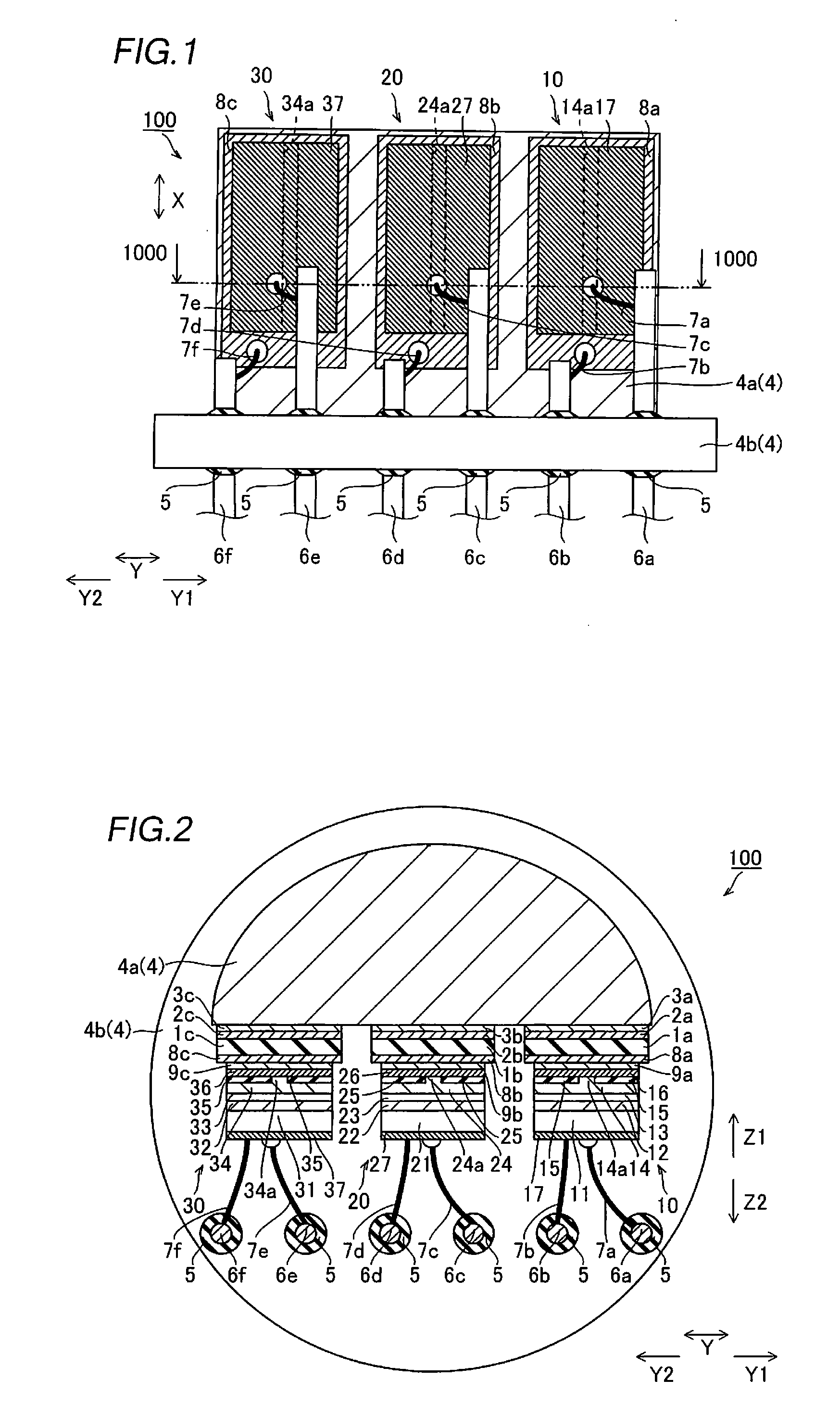
[0101]A modification of the first embodiment will be now described with reference to FIGS. 1, 6 and 7. In a laser diode device 200 according to the modification of the first embodiment, anode common connection in which positive electrodes (p-sides) are common is achieved by electrically connecting p-side electrodes 16, 26 and 36 to a support base 4a through conductive heat radiation substrates 201a, 201b and 201c, respectively, dissimilarly to the aforementioned first embodiment.
[0102]In the laser diode device 200 according to the modification of the first embodiment of the present invention, lead terminals 206a, 206c, 206e and 206g are mounted successively from a Y1 side on a conductive stem body 4b of a grounded package 4, as shown in FIGS. 6 and 7. First ends of wires 207a, 207c, 207e and 207g are connected to lead terminals 206a, 206c, 206e and 206g, respectively. As shown in FIG. 6, a second end of the wire 207g is connected to a surface of the cond
second embodiment
[0107]A second embodiment will be now described with reference to FIGS. 8 and 9. In a laser diode device 300 according to the second embodiment, blue and green laser diode elements 20 and 30 are bonded on a surface of the same heat radiation substrate 301d with a prescribed interval, dissimilarly to the aforementioned first embodiment. The heat radiation substrate 301d is an example of the “second heat radiation substrate” in the present invention.
[0108]In the laser diode device 300 according to the second embodiment of the present invention, the blue and green laser diode elements 20 and 30 are bonded on the surface of the heat radiation substrate 301d with the prescribed interval, as shown in FIGS. 8 and 9. More specifically, the heat radiation substrate 301d made of AlN having insulating properties and having high thermal conductivity is arranged to extend from a Y2 side of a support base 4a to the vicinity of a central portion in a direction Y, as shown in FIG. 9. The heat radiatio
third embodiment
[0111]A third embodiment will be now described with reference to FIGS. 10 and 11. In a laser diode device 400 according to a third embodiment, a monolithic blue and green two-wavelength laser diode element portion 460 is formed by blue and green laser diode elements 420 and 430, dissimilarly to the aforementioned second embodiment.
[0112]In the laser diode device 400 according to the third embodiment of the present invention, lead terminals 6a, 6b, 406d, 406h and 406f are mounted successively from a Y1 side on a stem body 4b of a package 4, as shown in FIG. 10. First ends of wires 7a, 7b, 407d, 407h and 407f are connected to the lead terminals 6a, 6b, 406d, 406h and 406f, respectively.
[0113]According to the third embodiment, the monolithic blue and green two-wavelength laser diode element portion 460 forms the blue and green laser diode elements 420 and 430, as shown in FIG. 11. More specifically, the blue laser diode element 420 has a structure in which an n-type cladding layer 422 mad
PUM
 Abstract
Description
Claims
Application Information
 - R&D Engineer
- R&D Manager
- IP Professional
- Industry Leading Data Capabilities
- Powerful AI technology
- Patent DNA Extraction
Browse by: Latest US Patents, China's latest patents, Technical Efficacy Thesaurus, Application Domain, Technology Topic.
© 2024 PatSnap. All rights reserved.Legal|Privacy policy|Modern Slavery Act Transparency Statement|Sitemap