Yield enhancement for stacked chips through rotationally-connecting-interposer
a technology of rotationally connecting interposers and stacked chips, which is applied in the direction of semiconductor/solid-state device testing/measurement, semiconductor/solid-state device details, instruments, etc., can solve the problems that the yield of stacked chips is low across the entire bonded structure, and the first and second wafers cannot be expected to produce functional stacked chips, etc., to achieve the highest stacked chip yield
- Summary
- Abstract
- Description
- Claims
- Application Information
AI Technical Summary
Benefits of technology
Problems solved by technology
Method used
Image

Examples
first embodiment
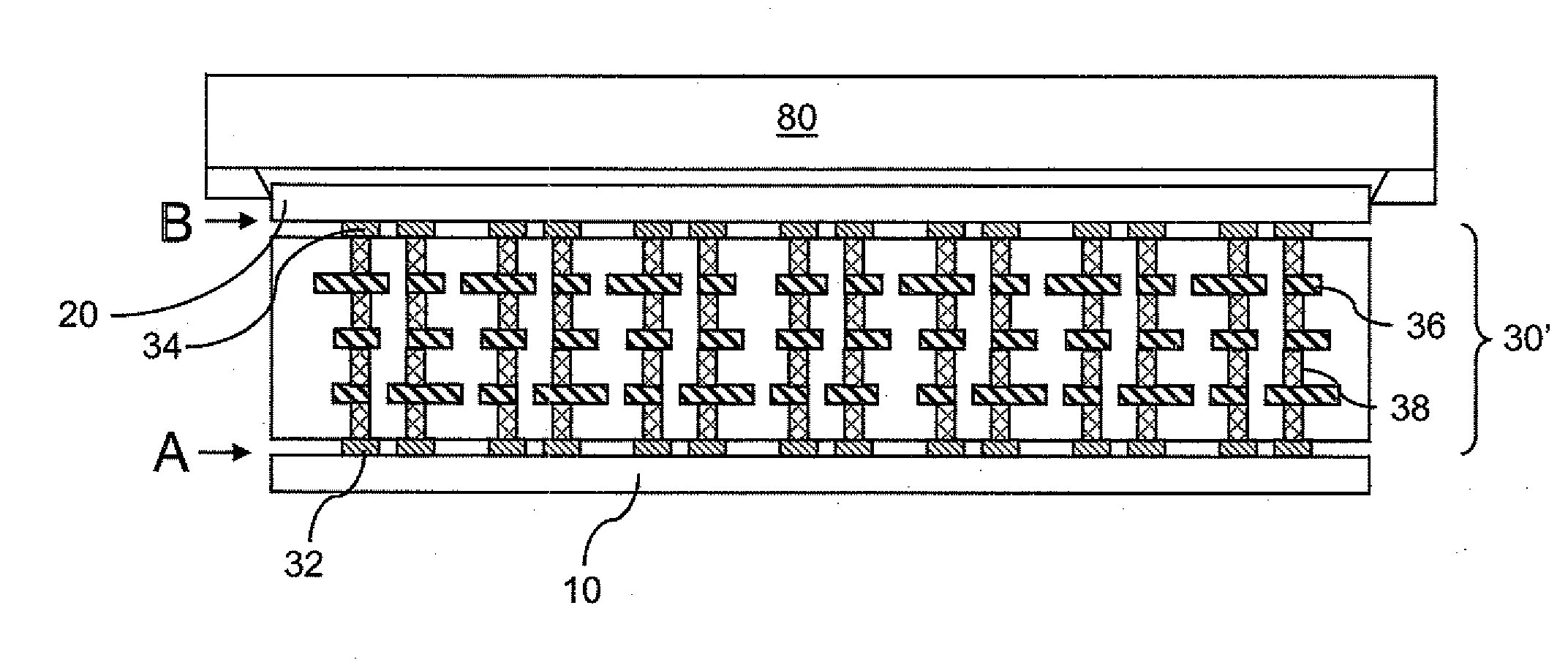
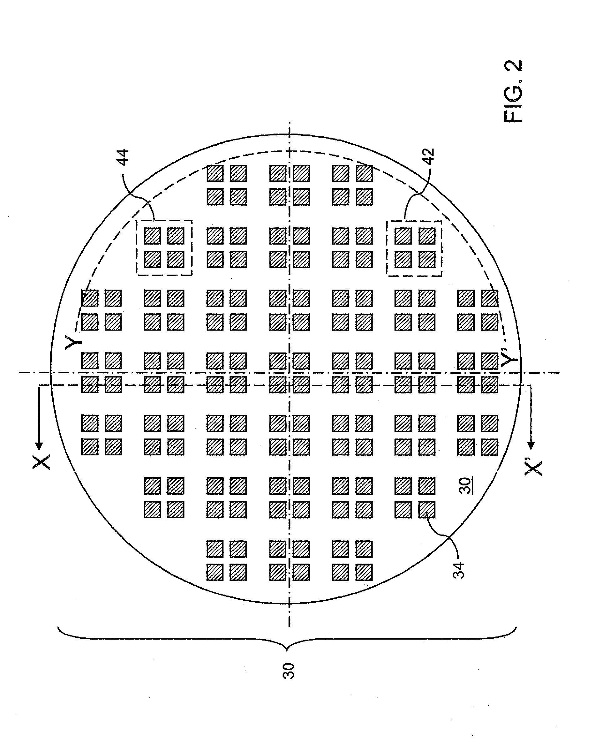
[0026]FIGS. 2-4 are various views of a first exemplary structure according to the present invention. The first exemplary structure includes a vertical stack, from bottom to top, of a first substrate 10, an interposer 30, and a second substrate 20. FIG. 2 is a top-down view of the first exemplary structure in which the second substrate 20 is not shown for clarity. FIG. 3 is a vertical cross-sectional view of the first exemplary structure along a flat vertical plane X-X′ shown in FIG. 2. FIG. 3 is a vertical cross-sectional view of the first exemplary structure along a curved vertical plane Y-Y′ shown in FIG. 2.
[0027]The first exemplary structure enables testing of a functionality that requires operation of a component in the first substrate 10 and another component in the second substrate 20 by providing electrical connections between the first substrate 10 and the second substrate 20 in the interposer 30. The interposer 30 enables testing of the combination of the first substrate 10 an
second embodiment
[0055]FIG. 12 a flow chart illustrates processing steps according to the present invention. Referring to step 410, an interposer is provided, which provides electrical connections between a first substrate and a second substrate. The interposer may provide electrical connections between the first and second substrates without any rotation between the first and second substrates, or may provide electrical connections between the first and second substrates with a rotational angle of (i−1) / N×2π in which N is an integer greater than 1, and i is an integer from 2 and N.
[0056]Referring to step 420, a first substrate including first semiconductor chips and a second substrate including second semiconductor chips are provided. The first semiconductor chips are arranged to have an N-fold rotational symmetry around a center axis of the first substrate. The second semiconductor chips are arranged to have an N-fold rotational symmetry around a center axis of the second substrate. Further, the fi
PUM
 Abstract
Description
Claims
Application Information
 - R&D Engineer
- R&D Manager
- IP Professional
- Industry Leading Data Capabilities
- Powerful AI technology
- Patent DNA Extraction
Browse by: Latest US Patents, China's latest patents, Technical Efficacy Thesaurus, Application Domain, Technology Topic.
© 2024 PatSnap. All rights reserved.Legal|Privacy policy|Modern Slavery Act Transparency Statement|Sitemap