Flash Memory Devices Having Multi-Bit Memory Cells Therein with Improved Read Reliability

Active Publication Date: 2011-08-11
SAMSUNG ELECTRONICS CO LTD
View PDF11 Cites 44 Cited by
  • Summary
  • Abstract
  • Description
  • Claims
  • Application Information

AI Technical Summary

Benefits of technology

[0007]The present disclosure provides a flash memory device and a read method thereof, which can ef

Problems solved by technology

However, as the number of bits programmed in each memory cell increase, the reliability decreases and the re

Method used


Image

  • Flash Memory Devices Having Multi-Bit Memory Cells Therein with Improved Read Reliability
  • Flash Memory Devices Having Multi-Bit Memory Cells Therein with Improved Read Reliability
  • Flash Memory Devices Having Multi-Bit Memory Cells Therein with Improved Read Reliability

Examples


Embodiment Construction

[0023]Preferred embodiments of the inventive concept will be described below in more detail with reference to the accompanying drawings. The inventive concept may, however, be embodied in different forms and should not be construed as limited to the embodiments set forth herein. Rather, these embodiments are provided so that this disclosure will be thorough and complete, and will fully convey the scope of the inventive concept to those skilled in the art. Like reference numerals refer to like elements throughout. The circuit configurations and the read operations of a flash memory device according to the inventive concept, which will be described below, are merely exemplary and various changes in form and details may be made therein without departing from the spirit and scope of the inventive concept.

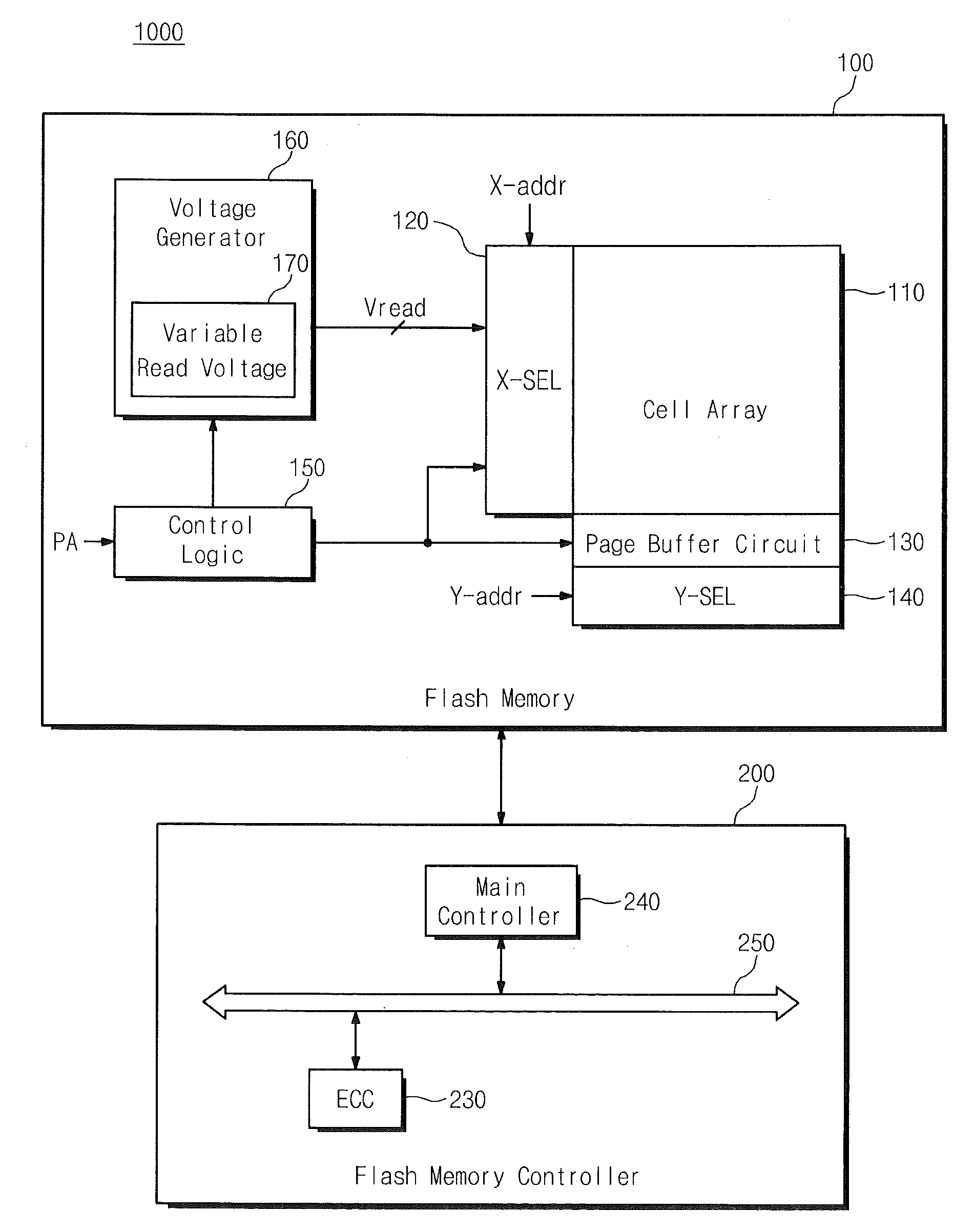
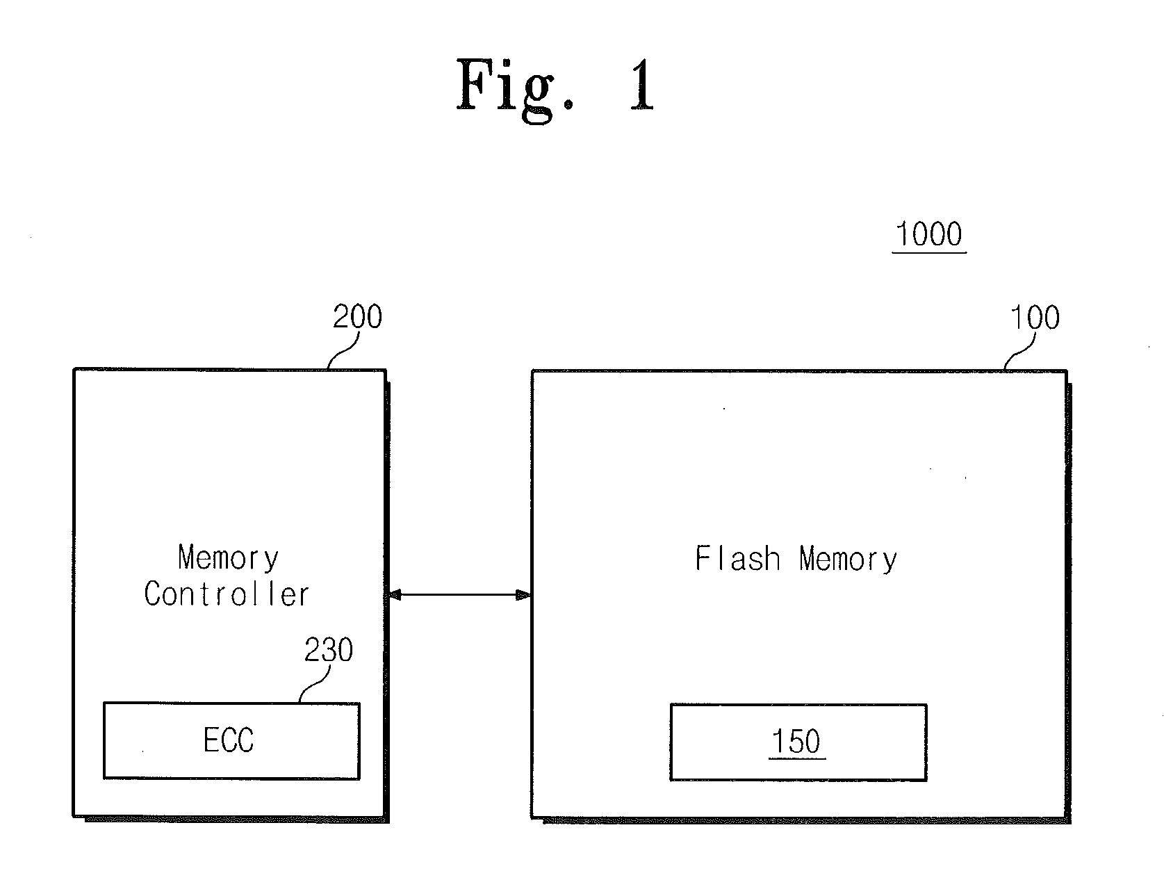
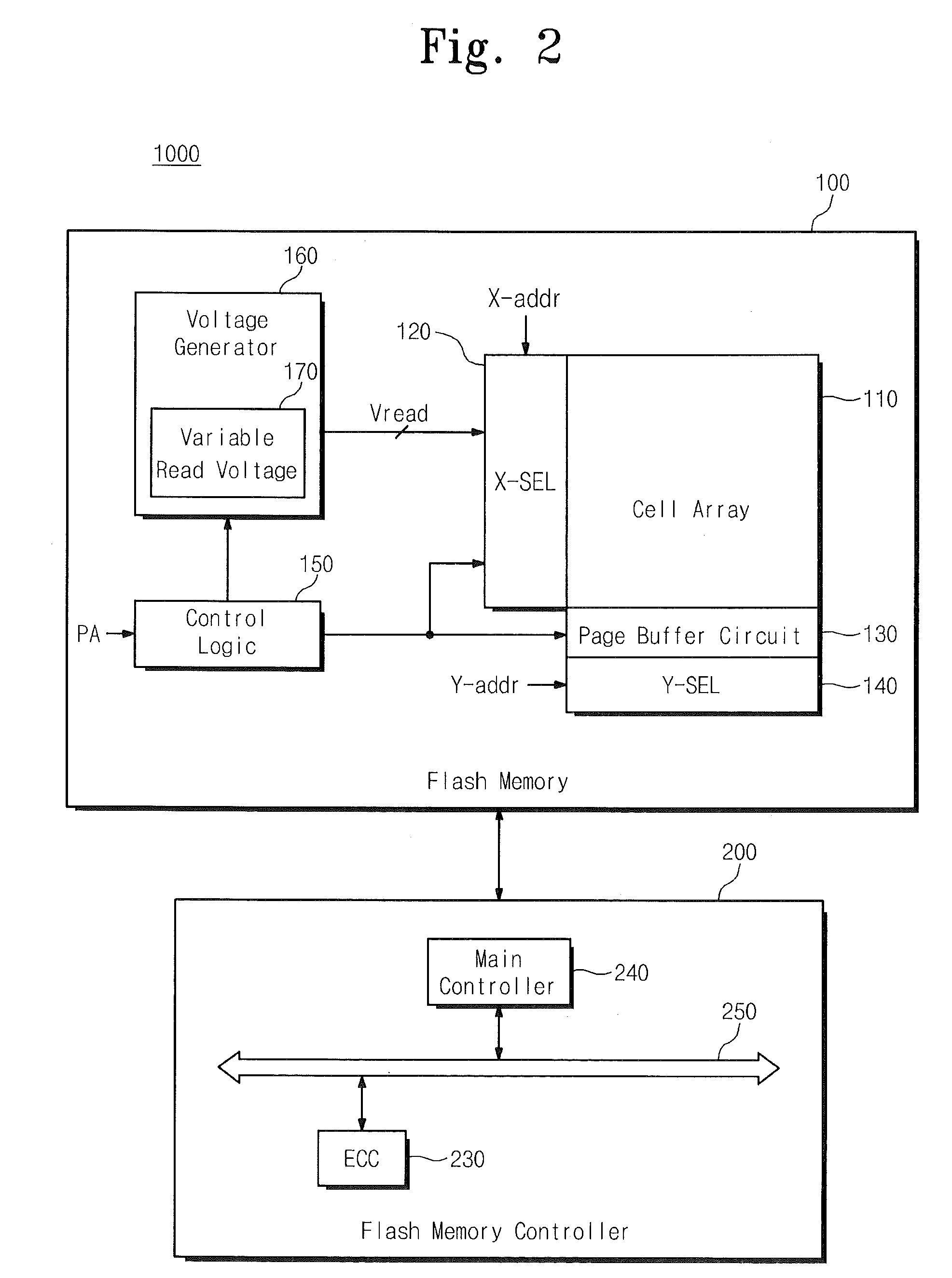
[0024]FIG. 1 is a diagram illustrating a schematic structure of a memory system 1000 including a flash memory 100 according to an exemplary embodiment of the inventive concept.

[0025]Referr


PUM


Abstract

Integrated circuit memory devices include an array of nonvolatile N-bit memory cells, where N is an integer greater than one. Control circuitry is also provided to reliably read data from the N-bit memory cells. This control circuitry, which is electrically coupled to the array, is configured to determine, among other things, a value of at least one bit of data stored in a selected N-bit memory cell in the array. This is done by decoding at least one hard data value and a plurality of soft data values (e.g., 6 data values) read from the selected N-bit memory cell using a corresponding plurality of unequal read voltages applied to the selected N-bit memory cell during a read operation.

Description


Claims


Application Information

Patent Timeline
Owner SAMSUNG ELECTRONICS CO LTD
Why Eureka
Try Eureka