Light-Emitting Device and Display Device
a technology of light-emitting devices and display devices, which is applied in the direction of semiconductor devices, diodes, electrical apparatus, etc., can solve the problems of difficult to increase yield or productivity, and achieve the effect of low power consumption
- Summary
- Abstract
- Description
- Claims
- Application Information
AI Technical Summary
Benefits of technology
Problems solved by technology
Method used
Image

Examples
embodiment 1
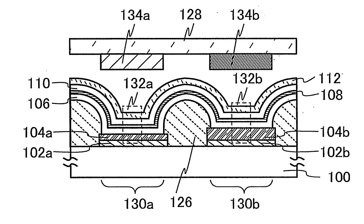
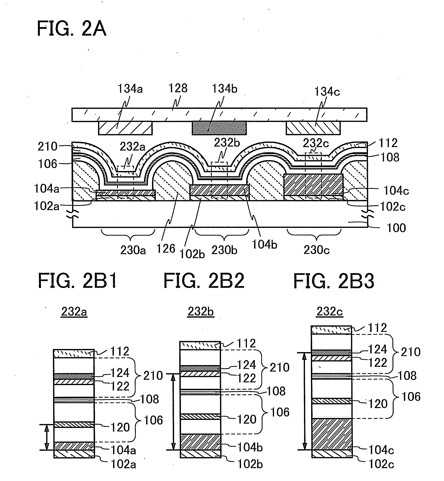
[0029]In this embodiment, one embodiment of an EL display device will be described with reference to FIGS. 1A and 1B, FIGS. 2A, 2B1, 2B2, and 2B3, and FIGS. 3A to 3C.
[0030]FIG. 1A is a cross-sectional view of a display portion in a display device of this embodiment. FIGS. 1B1 and 1B2 are enlarged views of part of the cross-sectional view of FIG. 1A.
[0031]The display device illustrated in FIG. 1A includes a first pixel 130a and a second pixel 130b. The first pixel 130a includes a first light-emitting element 132a provided over a substrate 100 and a first color filter layer 134a provided for a counter substrate 128 in a region overlapping with the first light-emitting element 132a. The second pixel 130b includes a second light-emitting element 132b provided over the substrate 100 and a second color filter layer 134b provided for the counter substrate 128 in a region overlapping with the second light-emitting element 132b.
[0032]In the display device illustrated in FIG. 1A, the first colo
embodiment 2
[0148]In this embodiment, an active matrix display device that is one embodiment of the present invention will be described with reference to FIGS. 4A and 4B. FIG. 4A is a plan view illustrating a display device. FIG. 4B is a cross-sectional view taken along line A-B and C-D in FIG. 4A
[0149]In the display device illustrated in FIGS. 4A and 4B, an element substrate 410 and a sealing substrate 404 are attached to each other with a sealant 405, and a driver circuit portion (a source-side driver circuit 401 and a gate side driver circuit 403) and a pixel port including a plurality of pixels are provided.
[0150]Note that a wiring 408 is a wiring for transmitting signals that are to be inputted to the source side driver circuit 401 and the gate side driver circuit 403, and receives a video signal, a clock signal, a start signal, a reset signal, and the like from a flexible printed circuit (FPC) 409 which serves as an external input terminal. Although only the FPC is illustrated here, a printe
embodiment 3
[0184]A display device disclosed in this specification can be applied to a variety of electronic appliances (including game machines). Examples of electronic devices include a television set (also referred to as a television or a television receiver), a monitor of a computer or the like, a camera such as a digital camera or a digital video camera, a digital photo frame, a mobile phone handset (also referred to as a mobile phone or a mobile phone device), a portable game console, a portable information terminal, an audio reproducing device, and a large-sized game machine such as a pachinko machine.
[0185]FIG. 5A illustrates a laptop personal computer, which includes a main body 3001, a housing 3002, a display port, a keyboard 3004, and the like. By applying the display device described in Embodiment 1 or 2 to the display port, the laptop personal computer can have a high level of definition and consumes a small amount of power.
[0186]FIG. 5B illustrates a personal digital assistant (PDA),
PUM
| Property | Measurement | Unit |
|---|---|---|
| Length | aaaaa | aaaaa |
| Thickness | aaaaa | aaaaa |
| Wavelength | aaaaa | aaaaa |
Abstract
Description
Claims
Application Information
 - R&D Engineer
- R&D Manager
- IP Professional
- Industry Leading Data Capabilities
- Powerful AI technology
- Patent DNA Extraction
Browse by: Latest US Patents, China's latest patents, Technical Efficacy Thesaurus, Application Domain, Technology Topic.
© 2024 PatSnap. All rights reserved.Legal|Privacy policy|Modern Slavery Act Transparency Statement|Sitemap