Wafer-Supporting Device and Method for Producing Same
- Summary
- Abstract
- Description
- Claims
- Application Information
AI Technical Summary
Benefits of technology
Problems solved by technology
Method used
Image
Examples
example 1
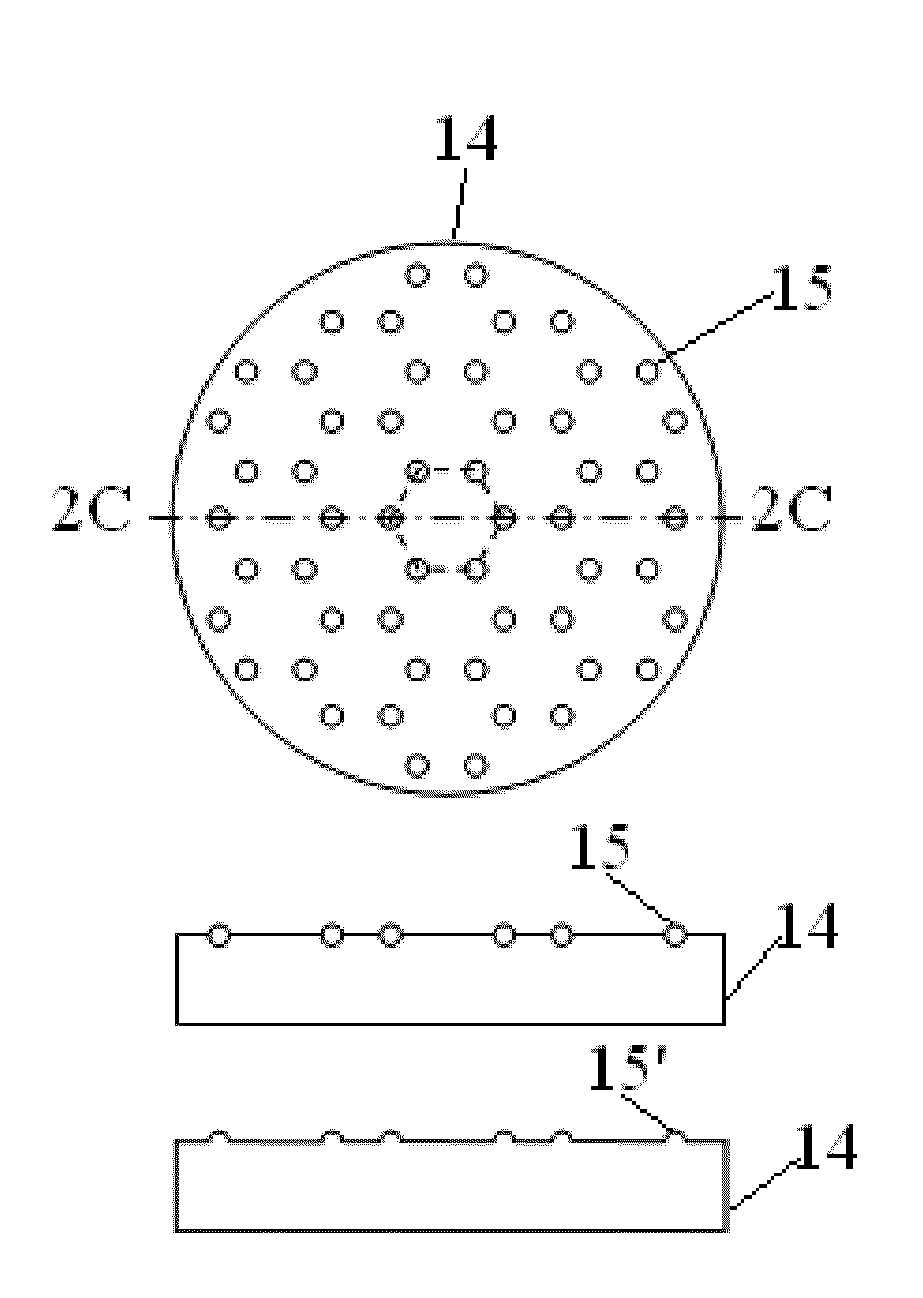
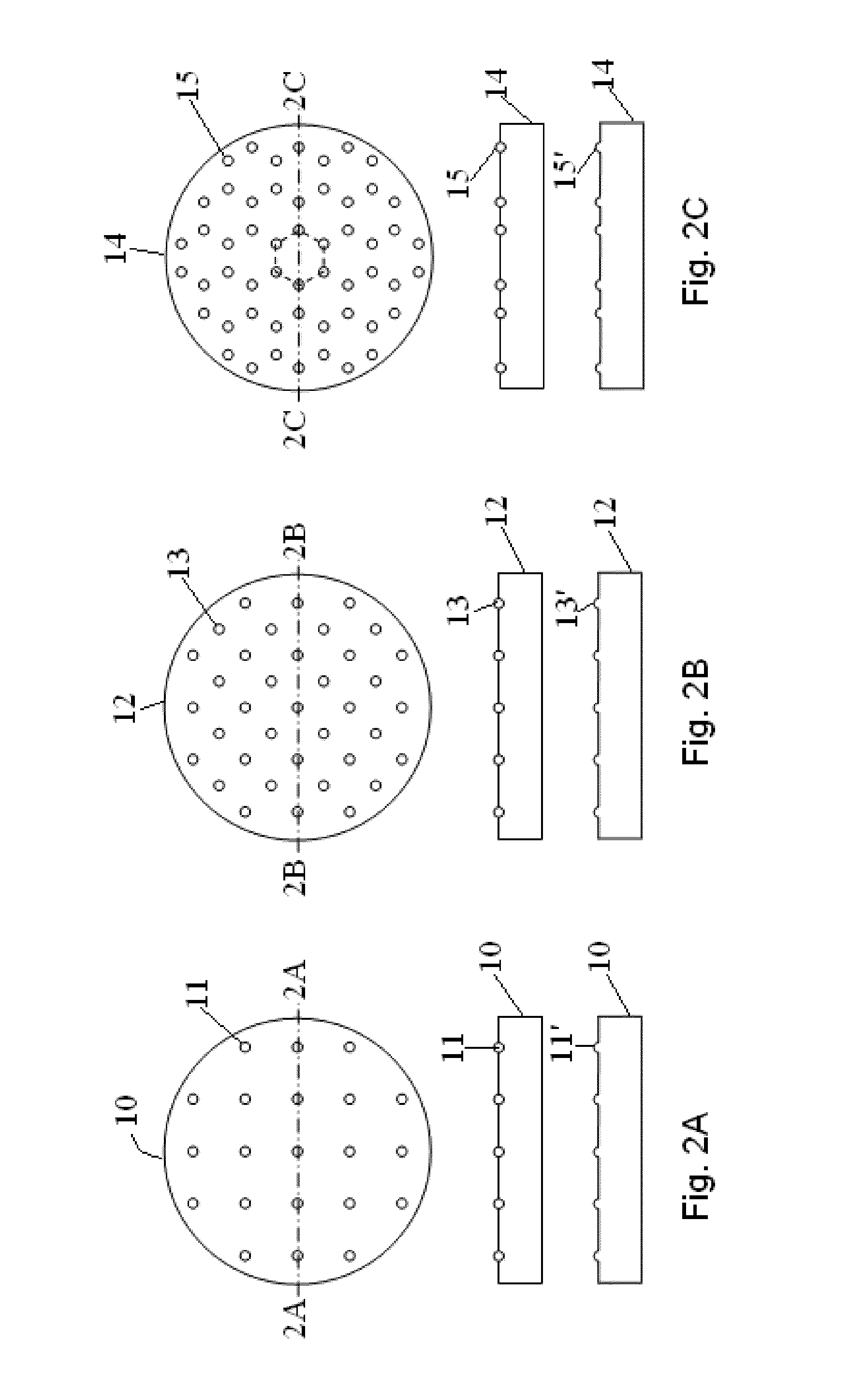
[0062]Film formation was conducted on a wafer in the same manner as in Comparative Example 1, except that a wafer-supporting device illustrated in FIG. 2B (37 protrusions) using sapphire balls having a diameter of 2 mm and a height (H′) of 50 μm (H=38 μm) was used. Due to the differences in thermal expansion coefficient between the aluminum alloy body and the sapphire balls, the height in use (H) was determined to be about 12 μm shorter than the height in non-use (H′) as calculated below:
A=CTE(M)(23E−6: aluminum alloy 6061)×D(M)(0.002 m)×(T1−T0)(T1=390° C., T0=25° C.)=17.0E−6 m
B=CTE(B)(7E−6: aluminum alloy 6061)×D(M)(0.002 m)×(T1−T0)(T1=390° C., T0=25° C.)=5.18E−6 m
A−B=11.8E−6 m
H=H′−11.8 [μm] (≈12 μm).
[0063]FIG. 4 is an image of Defect Review SEM (scanning electron microscope) of a scratched portion of the reverse side of the wafer after the film formation. FIG. 5 is an image of Defect Review SEM (scanning electron microscope) of a circular deformation portion of the reverse side of th
example 2
[0064]Film formation was conducted on a wafer in the same manner as in Example 1, except that a wafer-supporting device illustrated in FIG. 2A (21 protrusions) using sapphire balls having a diameter of 2 mm, and a wafer-supporting device illustrated in FIG. 2B (37 protrusions) using sapphire balls having a diameter of 2 mm were used, and the height (H′) of these wafer-supporting devices was changed as shown in FIG. 8, and film stress of the films was measured (due to the differences in thermal expansion coefficient between the aluminum alloy body and the sapphire balls, the height in use (H) was determined to be about 12 μm shorter than the height in non-use (H′)). FIG. 8 is a graph illustrating the relationship between the film stress and the height (H′) of protrusions according to this embodiment. The stress was the average of seven films, and the data when the height (H′) was 40 μm or less were obtained using the wafer-supporting device illustrated in FIG. 2A, and the data when the
example 3
[0065]Film formation was conducted on a wafer in the same manner as in Example 1, except that a wafer-supporting device illustrated in FIG. 2A (21 protrusions) using sapphire balls having a diameter of 2 mm, and a wafer-supporting device illustrated in FIG. 2B (37 protrusions) using sapphire balls having a diameter of 2 mm were used, and the height (H′) of these wafer-supporting devices was changed as shown in FIG. 9, and the number of particles on the reverse side of the wafer was measured. FIG. 9 is a graph illustrating the relationship between the number of particles on a reverse side of a wafer and the height (H′) of protrusions according to this embodiment. The number of particles was the average of three wafers. As shown in FIG. 9, when the height (H′) of the protrusions illustrated in FIG. 2A (21 protrusions) was no less than about 40 μm (H about 28 μm), the number of particles having a diameter of 0.2 μm or larger could be controlled to under about 300, whereas when the height
PUM
| Property | Measurement | Unit |
|---|---|---|
| Diameter | aaaaa | aaaaa |
| Diameter | aaaaa | aaaaa |
| Length | aaaaa | aaaaa |
Abstract
Description
Claims
Application Information
 - R&D Engineer
- R&D Manager
- IP Professional
- Industry Leading Data Capabilities
- Powerful AI technology
- Patent DNA Extraction
Browse by: Latest US Patents, China's latest patents, Technical Efficacy Thesaurus, Application Domain, Technology Topic.
© 2024 PatSnap. All rights reserved.Legal|Privacy policy|Modern Slavery Act Transparency Statement|Sitemap


