E-mode hfet device

Active Publication Date: 2013-06-27
QUALCOMM INC
View PDF11 Cites 58 Cited by
  • Summary
  • Abstract
  • Description
  • Claims
  • Application Information

AI Technical Summary

Benefits of technology

[0025]The present invention describes a transistor based on a Hetero junction FET structure, where the metal gate has been replaced by a stack formed by a highly doped compound semiconductor and an insulating layer in order to achieve enhancement mode operation and at the same time drastically reduce the gate current leakage. The combination of the insulating layer with a highly doped semiconductor allows the tuning of the threshold voltage of the device at the desired value by simply changing the composition of

Problems solved by technology

However the need to further improve its general performance while reducing its cost is still a necessity that poses a significant challenge.
However, the reduction of Lg alone does not lead to maximum RF performance.
Another important limitation of these structures is the difficulty to make them operate in enhancement mode.
The enhancement behavior of the previous structure has also another disadvantage: in order to isolate the source and the drain terminals from the gate, the gate region must be made smaller than the etched region formed in the barrier layer, leaving two isolating regions 9 and 7 at the sides of the gate.
This causes a discontinuity in the doping modulation of the channel, adding two extra resistive paths in the channel.
HEMT employing polar materials such as GaN and III-Nitride alloys oriented along the direction, present similar limitations.
This is due to the lack of stable metal alloys with high work-function to be used as gate electrode.
This solution therefore degrades the ca

Method used


Image

  • E-mode hfet device
  • E-mode hfet device
  • E-mode hfet device

Examples


Embodiment Construction
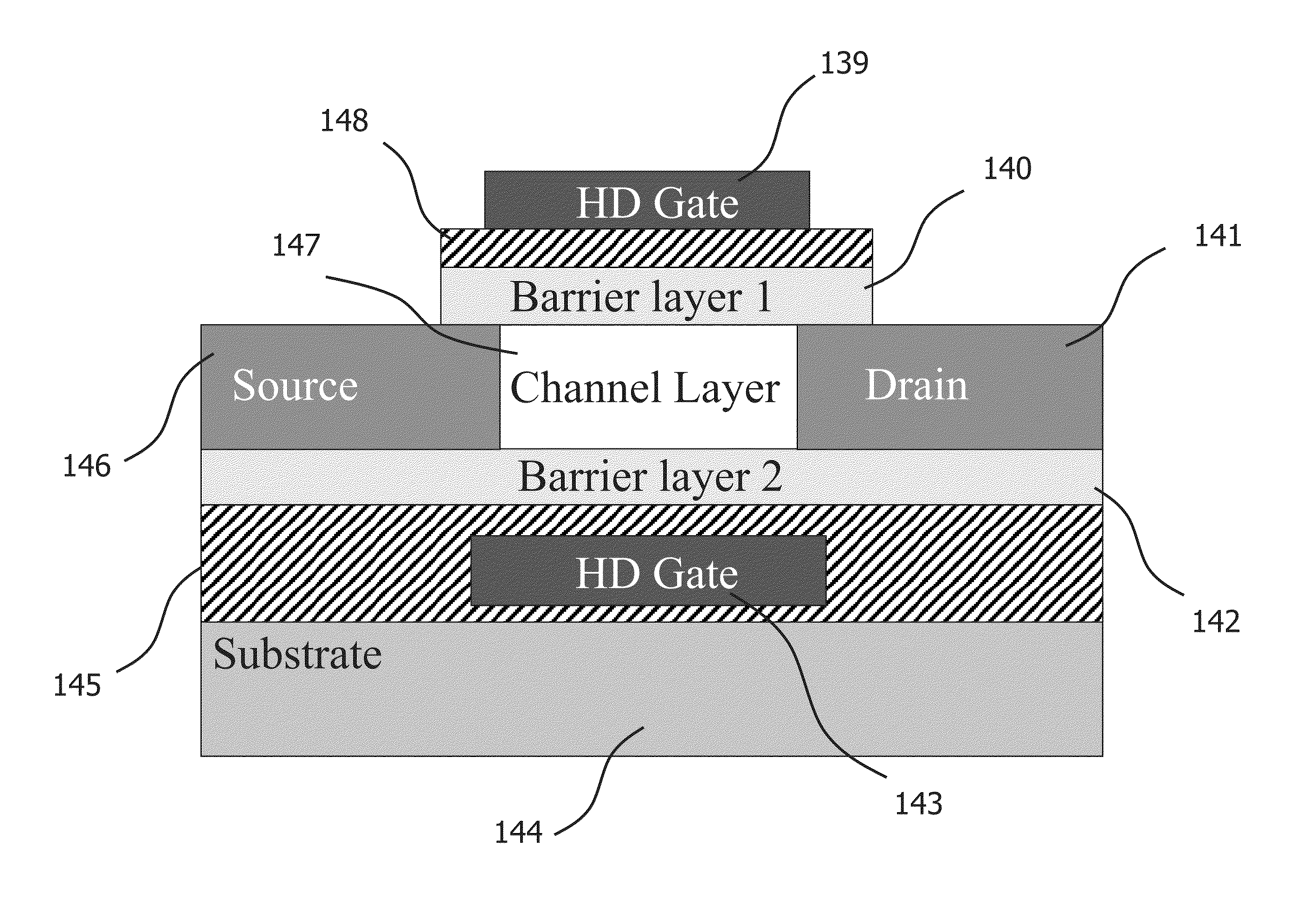
A FIG. 4

[0077]FIG. 4 is showing a Hetero-structure FET (HFET) device according to the preferred embodiment of the invention. The metallic or n+-type semiconductor regions 28 and 25 define the source and the drain of the transistor. Regions 29 corresponds to the barrier layer of the device, and the channel layer 27 is the region where the electron (or hole)—channel is formed. Region 23, which is formed by a heavily doped semiconductor layer on the top of an insulating layer 24, corresponds to the gate of the device.

[0078]If the desired device is an n-channel HFET, the channel region should have an electron affinity greater with respect to the barrier layer 29, in order to confine the carrier transport inside the layer 27 during the normal operation of the device. The gate region 23 instead, can be built with the same, greater or lower electron affinity with respect to the barrier layers, depending on the desired device characteristics. If necessary, the gate 23 and / or the barrier laye


PUM


Abstract

The present invention describes a transistor based on a Hetero junction FET structure, where the metal gate has been replaced by a stack formed by a highly doped compound semiconductor and an insulating layer in order to achieve enhancement mode operation and at the same time drastically reduce the gate current leakage. The combination of the insulating layer with a highly doped semiconductor allows the tuning of the threshold voltage of the device at the desired value by simply changing the composition of the semiconductor layer forming the gate region and/or its doping allowing a higher degree of freedom. In one of the embodiment, a back-barrier layer and a heavily doped threshold tuning layer are used to suppress Short Channel Effect phenomena and to adjust the threshold voltage of the device at the desired value. The present invention can be realized both with polar and non-polar (or semi-polar) materials.

Description


Claims


Application Information

Patent Timeline
Owner QUALCOMM INC
Why Eureka
Try Eureka