Semiconductor structures provided within a cavity and related design structures

Active Publication Date: 2014-02-27
WISPRY INC +1
View PDF3 Cites 5 Cited by
  • Summary
  • Abstract
  • Description
  • Claims
  • Application Information

AI Technical Summary

Benefits of technology

[0009]In yet another aspect of the invention, a structure comprises a beam structure located within a cavity. The structure further comprises at least one vent hole positioned over a free end of the beam structure. The at least one vent hole having a first size which prevents or minimizes material deposition on the free end of the beam structure. The structure further comprises at least another vent hole positioned over a fixed end of the beam structure, the at least another vent hole having a second size, larger than the first size.

Problems solved by technology

However, it has been found that in conventional processes the sealing material deposits on the free end (moving end) of the cantilever beam, which significantly changes the stress gradient of the beam and affects the MEMS performance.
Illustratively, the material on the free end of the cantilever beam can affect the pull-in voltage, the zero voltage capacitance of the beam, e.g., make the Cmin unstable, in addition to inadvertently causing actuation of the MEMS structure, upon the application of an RF signal.
In still additional problems, it has been found that some cavity sealing techniques distort the beam shape and significantly affects beam shape variability.
Another problem which has been identified is degraded MEMS cycling properties and MEMS beam bounce after switching.

Method used


Image

  • Semiconductor structures provided within a cavity and related design structures
  • Semiconductor structures provided within a cavity and related design structures
  • Semiconductor structures provided within a cavity and related design structures

Examples


Example

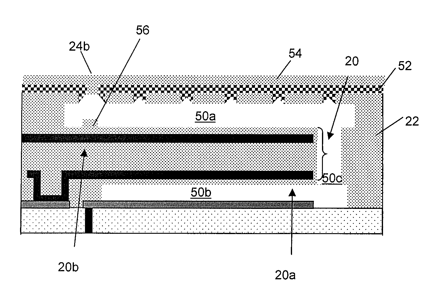
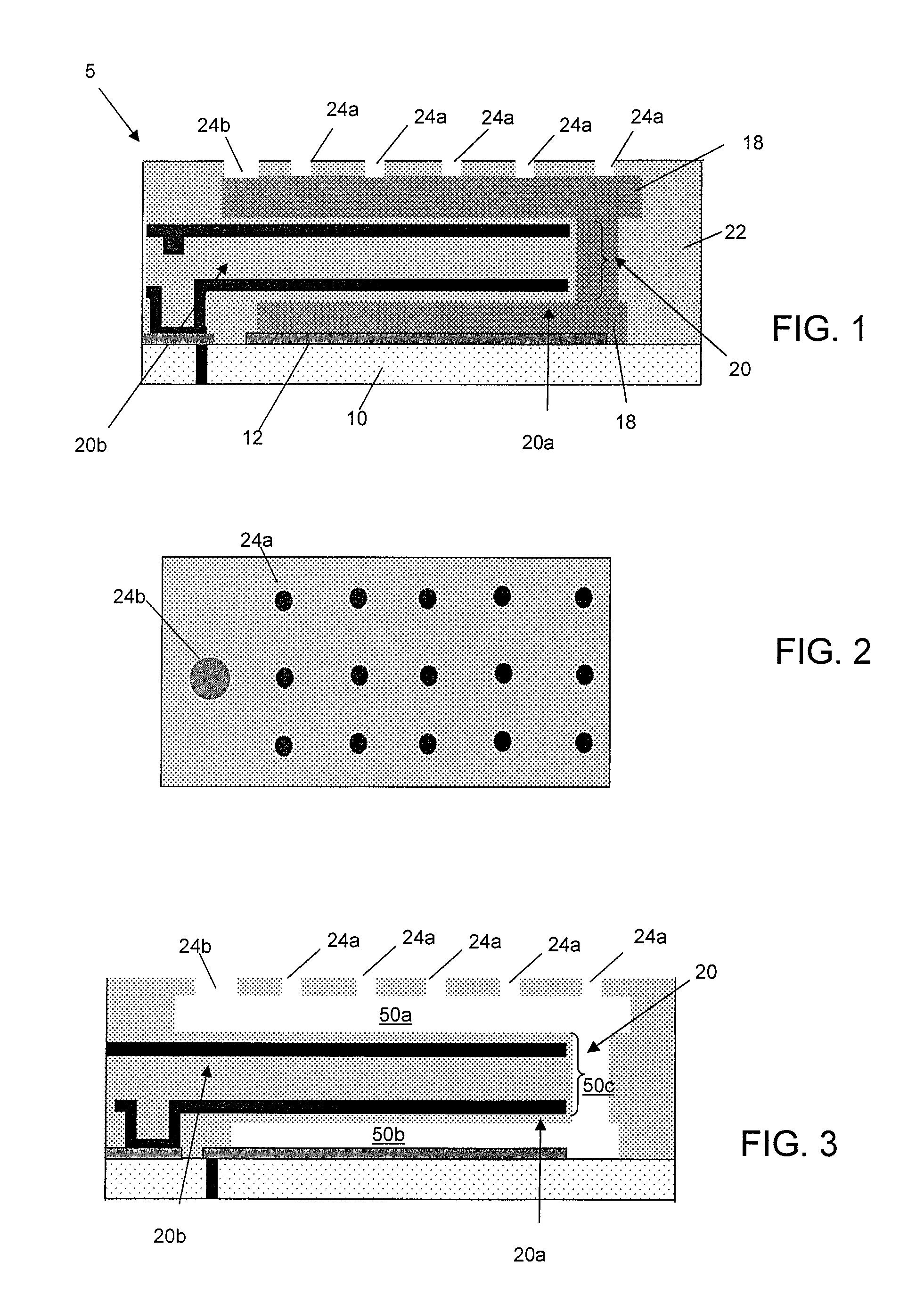
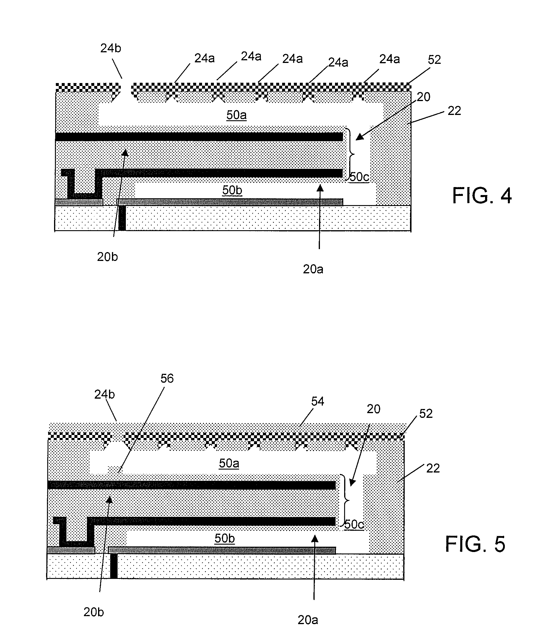
[0018]The invention relates to semiconductor structures and methods of manufacture and, more particularly, to structures provided within a cavity, methods of manufacture and design structures. In embodiments, the structures can be, for example, Micro-Electro-Mechanical System (MEMS) structures, accelerometers, filters, oscillators, resonators, acoustic wave devices, etc., any of which can be provided within a sealed cavity structure. Advantageously, the methods of forming the structures of the present invention significantly reduce material variability on the structure, e.g., MEMS beam, itself. In one example, the reduction of material variability on the beam solves many of the issues which have now been found to exist with MEMS structures, including, for example, providing the following advantages:

[0019](i) stabilizing pull-in voltage issues and Cmin;

[0020](iii) preventing inadvertent actuation of the MEMS structure, upon the application of an RF signal;

[0021](iii) significantly reduc


PUM


Abstract

Micro-Electro-Mechanical System (MEMS) structures, methods of manufacture and design structures are disclosed. The method includes forming at least one Micro-Electro-Mechanical System (MEMS) cavity. The method for forming the cavity further includes forming at least one first vent hole of a first dimension which is sized to avoid or minimize material deposition on a beam structure during sealing processes. The method for forming the cavity further includes forming at least one second vent hole of a second dimension, larger than the first dimension.

Description


Claims


Application Information

Patent Timeline
Owner WISPRY INC
Why Eureka
Try Eureka