Capacitive touch panel

Active Publication Date: 2015-03-12
TRENDON TOUCH TECHNOLOGY CORPORATION
View PDF3 Cites 4 Cited by
  • Summary
  • Abstract
  • Description
  • Claims
  • Application Information

AI Technical Summary

Benefits of technology

[0006]In the prior art, a conventional capacitive touch panel is affected by different refraction indexes of a variety of interface materials when light is transmitted through it. Therefore, its sensing electrodes tend to emerge on the surface of the capacitive touch panel. In addition, since a variety of regions on the capacitive touch panel are res

Problems solved by technology

As a result, the brightness is non-uniform on the surface of the capacitive touch panel.
To be brief, the conventional capacitive touch panel often has the drawback of poor optical performance.
In such a

Method used


Image

  • Capacitive touch panel
  • Capacitive touch panel
  • Capacitive touch panel

Examples


first embodiment

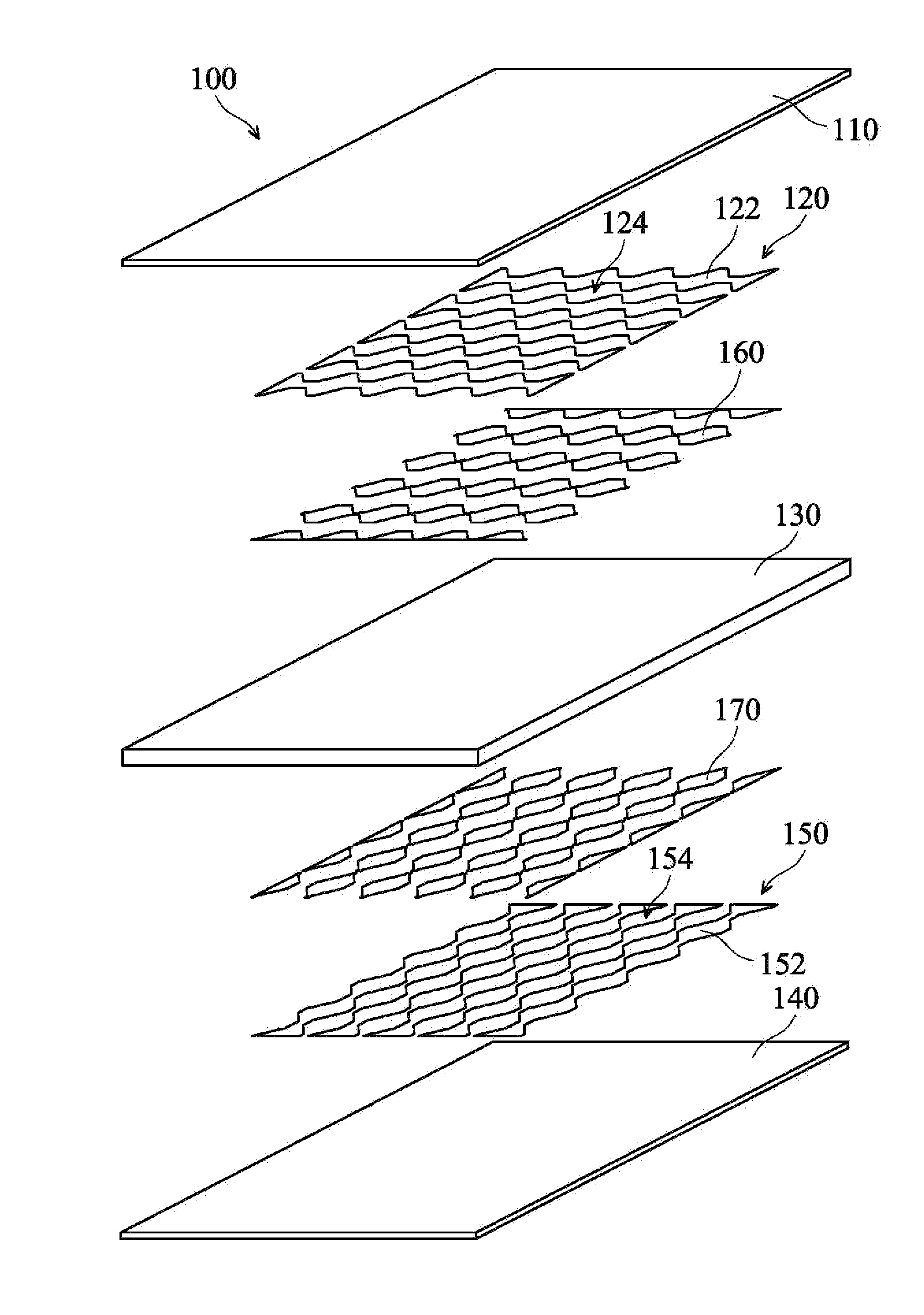
[0044]In the first embodiment relative to the capacitive touch panel 100, the second sensing electrode serials 150 are disposed in a second direction on the top surface of the second transparent substrate 140. Each second sensing electrode serial 150 is formed by cascading second sensing electrodes 152, each of which substantially has a diamond shape. The second sensing electrode serials 150 are made of transparent conductive materials, such as ITO (Indium Tin Oxide), AZO (Aluminum-doped Zinc Oxide), IZO (Indium Zinc Oxide), nanosilver films, CNT (Carbon Nanotube), or graphene films. The second sensing electrode serials 150 are formed on the surface of the second transparent substrate 140 through etching, printing, or sputtering processes. Each second hollow region 154 is formed between two adjacent second sensing electrodes 152. The second direction is perpendicular to the aforementioned first direction.

[0045]FIG. 4A is a diagram for illustrating a sectional view of the capacitive tou

fifth embodiment

[0051]In the fifth embodiment relative to the capacitive touch panel 500, the second sensing electrode serials 550 are disposed in a second direction on the top surface of the second transparent substrate 540. Each second sensing electrode serial 550 is formed by cascading second sensing electrodes 552, each of which substantially has a diamond shape. The second sensing electrode serials 550 are made of transparent conductive materials, such as ITO (Indium Tin Oxide), AZO (Aluminum-doped Zinc Oxide), IZO (Indium Zinc Oxide), nanosilver films, CNT (Carbon Nanotube), or graphene films. The second sensing electrode serials 550 are formed on the surface of the second transparent substrate 540 through etching, printing, or sputtering processes. Each second hollow region 554 is formed between two adjacent second sensing electrodes 552. The second direction is perpendicular to the aforementioned first direction.

[0052]Please further refer to FIG. 12A. FIG. 12A is a diagram for illustrating a s


PUM


Abstract

A capacitive touch panel includes a first transparent substrate, a second transparent substrate, and an isolation layer. First and second sensing electrode serials are disposed on surfaces of the first and second transparent substrates, respectively. The first sensing electrode serials are formed by cascading first sensing electrodes. A first hollow region is formed between two adjacent first sensing electrodes. A first compensating electrode is formed in the first hollow region on the surface of the first transparent substrate. The second sensing electrode serials are formed by cascading second sensing electrodes. A second hollow region is formed between two adjacent second sensing electrodes. A second compensating electrode is formed in the second hollow region on the surface of the second transparent substrate. The isolation layer is disposed between the first and second transparent substrates.

Description


Claims


Application Information

Patent Timeline
Owner TRENDON TOUCH TECHNOLOGY CORPORATION
Why Eureka
Try Eureka