Display panel and display device
a display panel and display panel technology, applied in the field of display panel and display device, can solve the problems of weaker electric field intensity of the notch, uncontrollable rotation thereof, and image retention problem, so as to avoid image retention problem, enhance response ability of the lc, and improve the surface roughness of the first part
- Summary
- Abstract
- Description
- Claims
- Application Information
AI Technical Summary
Benefits of technology
Problems solved by technology
Method used
Image

Examples
Embodiment Construction
[0027]The present invention will be apparent from the following detailed description, which proceeds with reference to the accompanying drawings, wherein the same references relate to the same elements.
[0028]The display panel of the invention can be an in-plane switch (IPS) LCD panel, a fringe field switching (FFS) LCD panel, a vertical alignment mode (VA mode) LCD panel, a photo alignment mode (PA mode) LCD panel, or a 3D LCD panel, but the invention is not limited thereto.
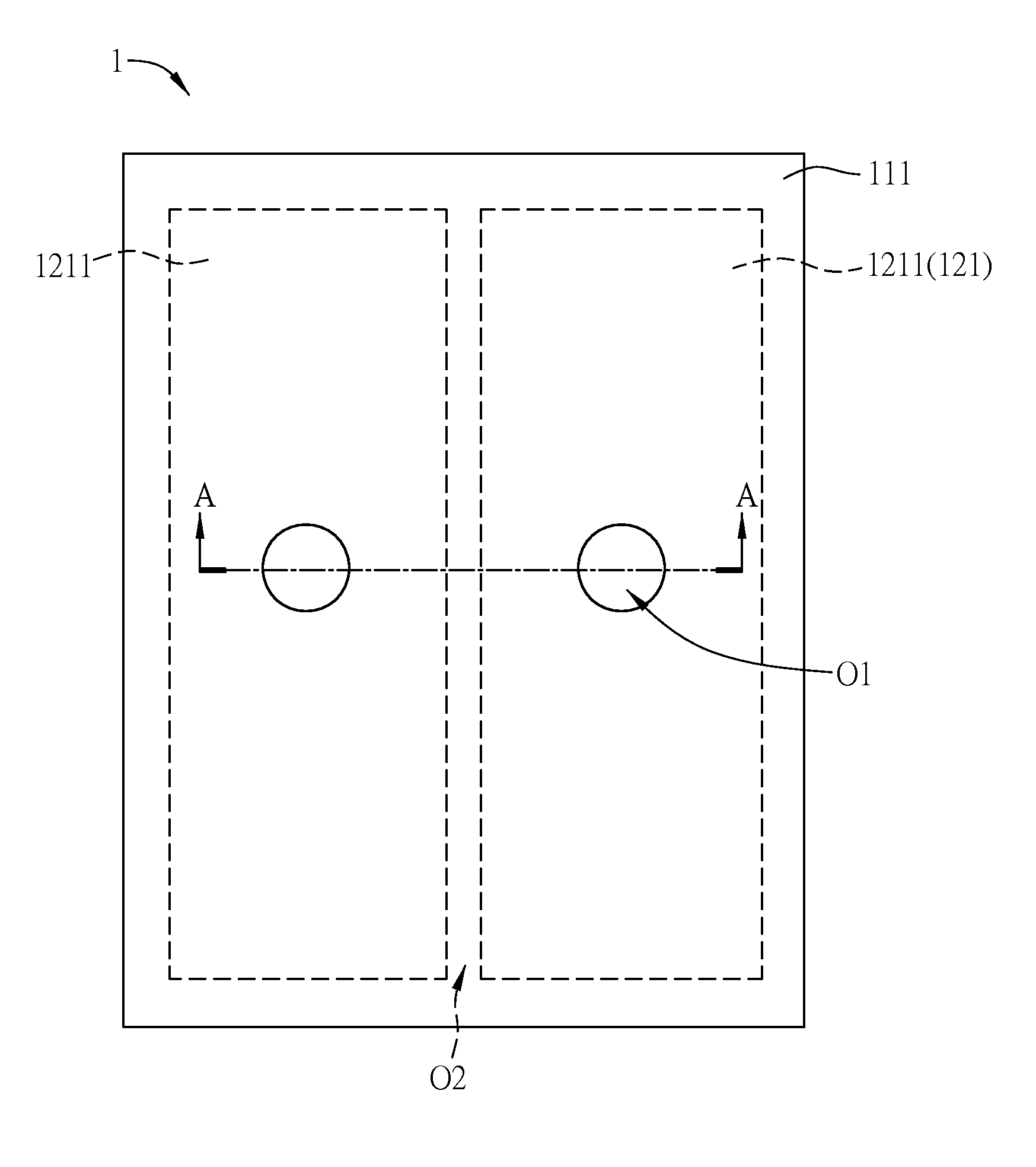
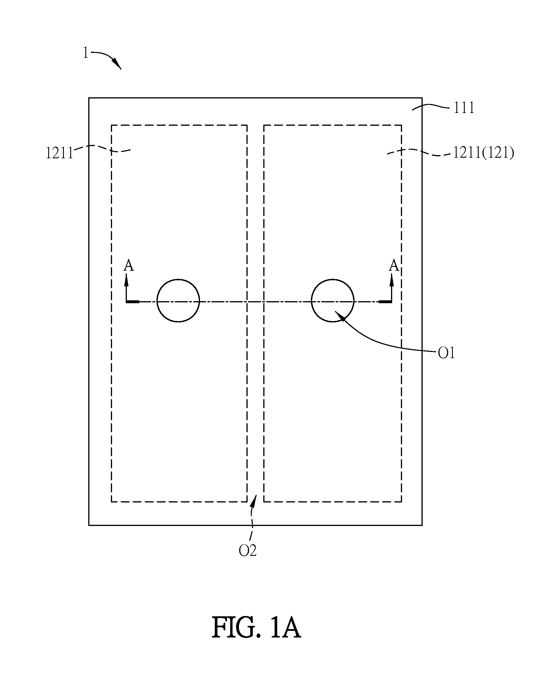
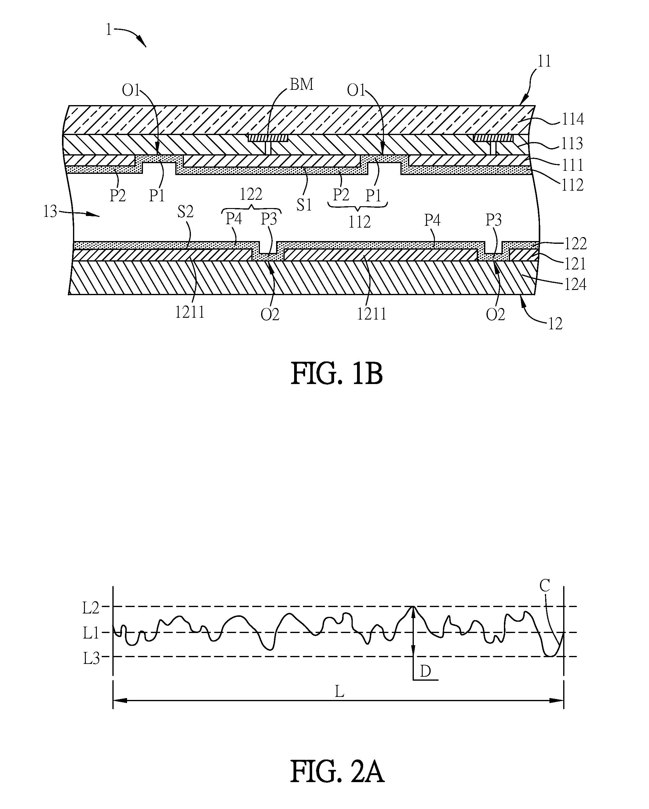
[0029]FIG. 1A is a schematic top view of a display panel 1 according to a preferred embodiment of the invention, and FIG. 1B is a schematic sectional diagram of the display panel 1 taken along the line A-A in FIG. 1. For clearly showing the relationship between the elements of the display panel 1, FIG. 1A just shows the first transparent conductive layer 111 and the first notch O1 of the first substrate 11, and the two adjacent transparent conductive portions 1211 of the second transparent conductive layer 121 of th
PUM
 Abstract
Description
Claims
Application Information
 - R&D Engineer
- R&D Manager
- IP Professional
- Industry Leading Data Capabilities
- Powerful AI technology
- Patent DNA Extraction
Browse by: Latest US Patents, China's latest patents, Technical Efficacy Thesaurus, Application Domain, Technology Topic.
© 2024 PatSnap. All rights reserved.Legal|Privacy policy|Modern Slavery Act Transparency Statement|Sitemap