Nitride semiconductor device and fabricating method thereof

a technology of nitride semiconductor and fabrication method, which is applied in the direction of semiconductor devices, basic electric elements, electrical appliances, etc., can solve the problems of increasing the importance of handling the leakage current level and the difficulty of producing high-power nitride semiconductor devices, so as to reduce the breakdown voltage and minimize the increase in leakage current

Active Publication Date: 2015-07-16
LG ELECTRONICS INC
View PDF4 Cites 9 Cited by
  • Summary
  • Abstract
  • Description
  • Claims
  • Application Information

AI Technical Summary

Benefits of technology

The technical effect that this patented technology provides for improving the performance of gallium-nitrides (gallium arsenide)-based transistors by reducing their resistance at high voltages while maintaining good conduction properties through use of specific layers or compositions on top of each other's surface. This results in improved efficiency and reliability during operation over time.

Problems solved by technology

This patents discusses challengings faced by future electronic components including gallium oxide based materials because they have higher electrical conductivity than traditional ones. These technical issues can lead to reduced reliability or even failure during long hours operating conditions without compromising their effectiveness.

Method used


Image

  • Nitride semiconductor device and fabricating method thereof
  • Nitride semiconductor device and fabricating method thereof
  • Nitride semiconductor device and fabricating method thereof

Examples


Embodiment Construction

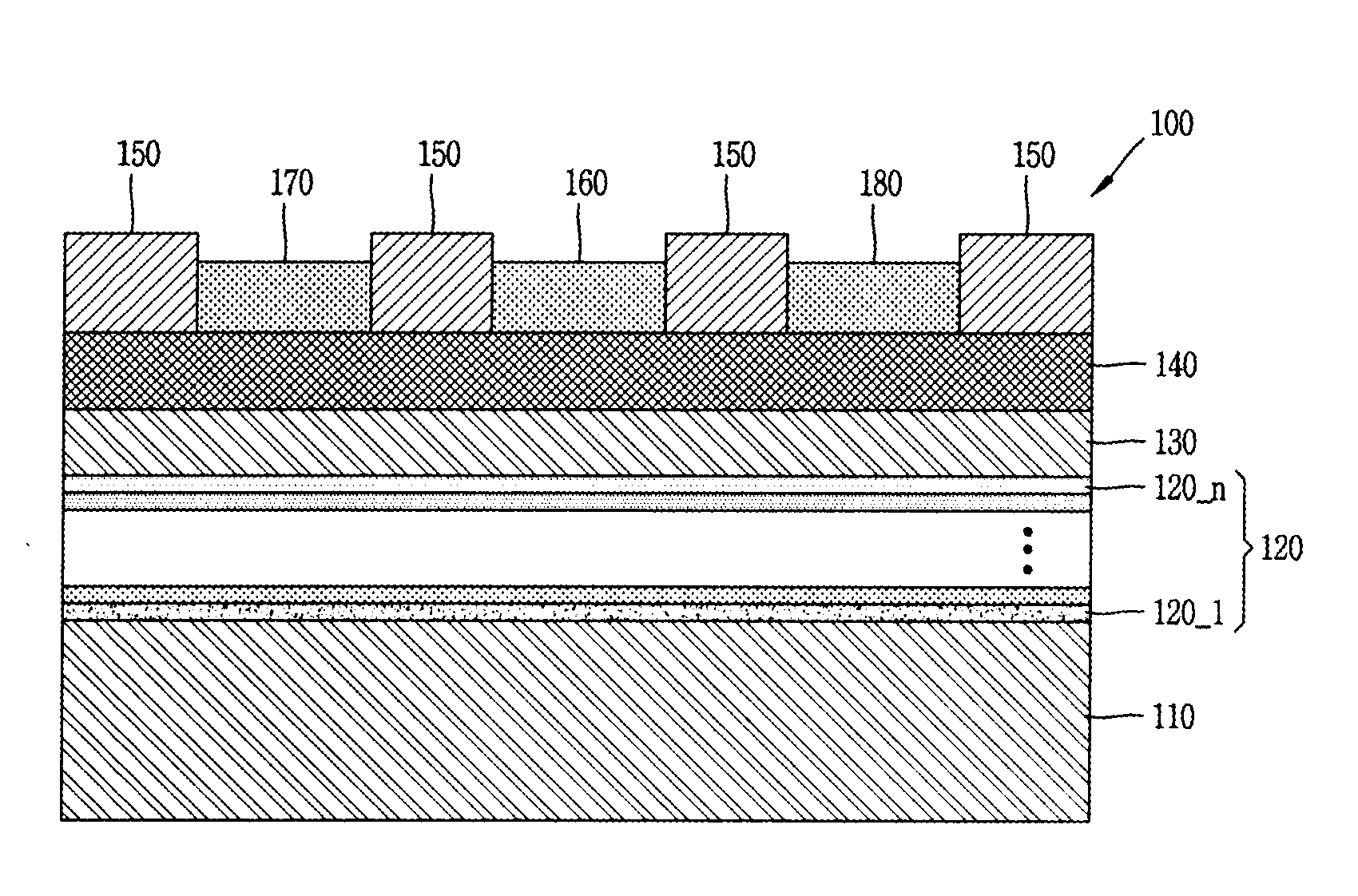
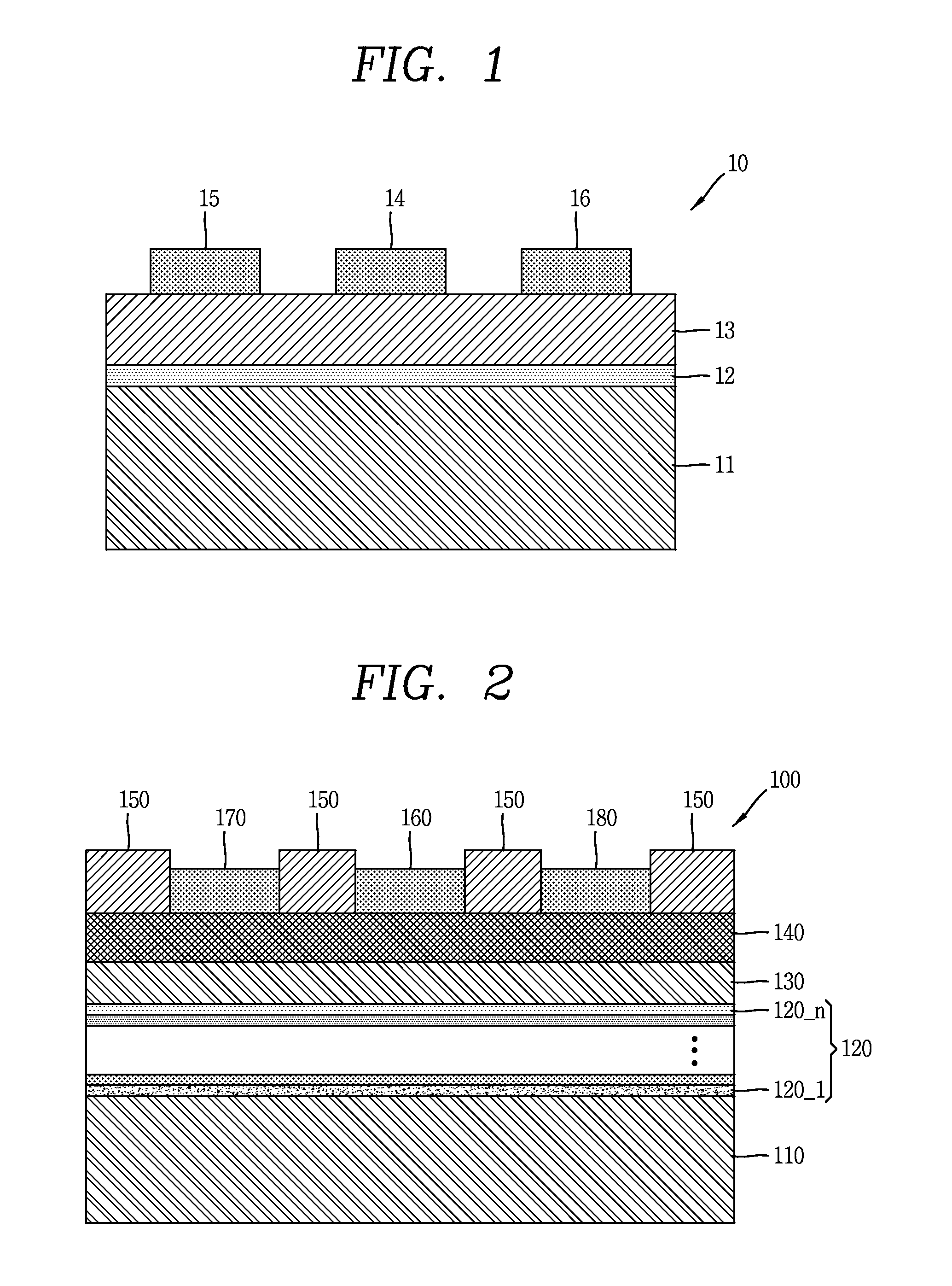
[0062]The technology disclosed herein may be applied to a Heterojunction Field Effect Transistor (HFET) and a fabricating method thereof. The technology disclosed herein is not limited to this, and may also be applicable to all kinds of application fields of nitride semiconductor devices and fabricating methods thereof to which the technological spirit of the technology can be applied.

[0063]Recently, a light-emitting diode (LED) including red wavelength bands in ultraviolet rays and a reddish-blue laser diode have been completely developed according to a growth technique of a nitride semiconductor, and are being widely used for traffic lights, electric signs, mobile phones and the like.

[0064]A power device using the nitride semiconductor has fast switching speed, an excellent withstanding voltage and fast current saturation speed, as compared with an Si-based device, and thus has many advantages for high-output high-voltage rather than the Si-based semiconductor devices.

[0065]That is,


PUM


Abstract

A nitride semiconductor power device includes an AlGaN multilayer, which has changeable Al composition along a depositing direction, and SixNy layer, so as to minimize an increase in a leakage current and a decrease in a breakdown voltage, which are caused while fabricating a heterojunction type HFET device. A semiconductor device includes a buffer layer, an AlGaN multilayer formed on the buffer layer, a GaN channel layer formed on the AlGaN multilayer, and an AlGaN barrier layer formed on the AlGaN multilayer, wherein aluminum (Al) composition of the AlGaN multilayer changes along a direction that the AlGaN multilayer is deposited.

Description


Claims


Application Information

Patent Timeline
Owner LG ELECTRONICS INC
Why Eureka
Try Eureka