High power impatt diode

Inactive Publication Date: 2001-06-26
CREE SWEDEN
View PDF11 Cites 7 Cited by
  • Summary
  • Abstract
  • Description
  • Claims
  • Application Information

AI Technical Summary

Benefits of technology

According to another preferred embodiment of the invention said means comprises a thin n-type layer with a substantially higher doping concentration than the drift layer arranged in the drift layer at a distance from said junction for locally increasing the electric field in a region of the drift,layer between said thin layer and the junction with respect to the average electric field in the drift layer. Such a thin layer with a higher doping concentration will result in a high, nearly constant electric field and accordingly a well defined avalanche region between said junction and said thin layer. The breakdown voltage of the diode may in this way be lowered substantially.
According to another preferred embodiment of the invention the distance between said junction and said thin layer is short with respect to the thickness of the drift layer, preferably less than 1 / 5, and most preferred less than 1 / 10 thereof. It has been found that the current required to achieve the avalanche resonance at a given frequency is rapidly decreased with a decreasing distance between the junction and the thin layer, which makes it easier to arrive to a negative differential resistance operation mode, i.e. operation with a frequency close to the avalanche resonance frequency.
According to another preferred embodiment of the invention the doping concentration of said thin layer is at least an order of magnitude, preferably at least two orders of magnitude higher than the doping concentration of the drift layer. Such a high doping concentration will considerably reduce the breakdown voltage of the diode.
According to another preferred embodiment of the invention said thin layer is laterally separated from the periphery of the diode, and the lateral separation of said thin layer from the periphery of the diode is most preferably larger than the distance between said thin layer and said junction, i.e. the avalanche multiplication region. This prevents undesirable surface effects and current filamentation that could result from such effects, since the high field region will not intersect the crystal surface. The risk of early peripheral breakdown will also be considerably reduced.
According to another preferred embodiment of the invention said junction is a Schottky barrier junction formed by a metal layer applied next to the drift layer at a second of said electrodes, and according to a further development of this embodiment the drift layer is connected directly to a metal layer forming said first electrode. An elimination of the effect of neutral regions on the device performance is obtained by elimination of the ohmic contacts. The elimination of ohmic anode contact will increase the overall voltage drop at the device by the value of the contact potential. On the other hand, using the barrier anode contact instead of a combination of a highly doped n-type contact region and an ohmic contact will entirely eliminate the alternating current (AC) losses in the contact region and eventually improve the device efficiency.
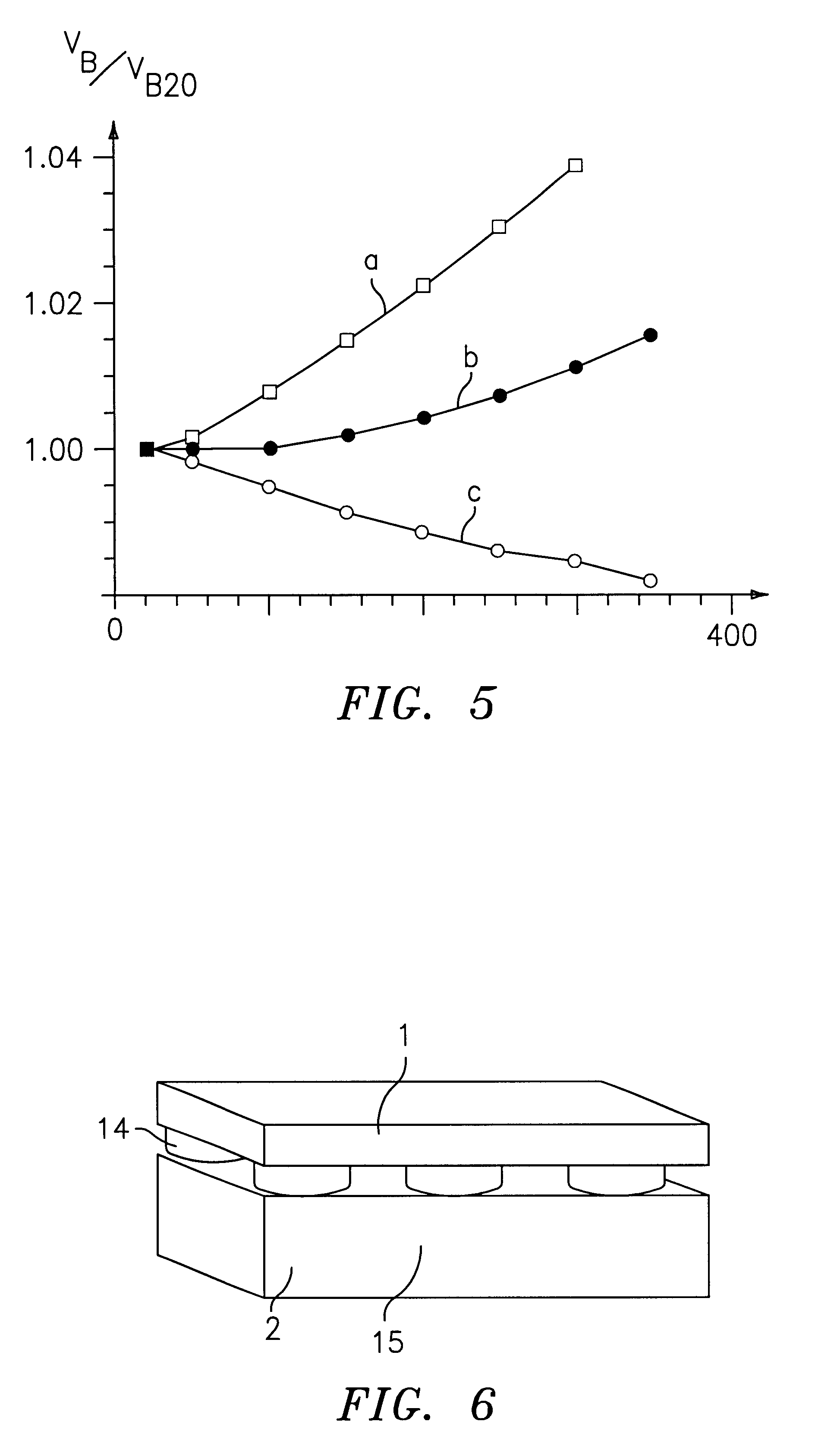
According to another preferred embodiment of the invention a diode is composed of an array of small sub-diodes with the characteristics defined mounted in parallel and laterally spaced onto a common heat sink. This will make it possible to obtain an efficiency of the dissipation of heat generated in an IMPATT diode of SiC being high enough. The individual sub-diodes have preferably a small diameter comparable to the thickness of the drift layer, so that the heat generated may be efficiently dissipated. It is preferred to make said heat sink of a material with a high thermal conductivity, such as diamond or electroplated gold.

Problems solved by technology

Such thermal limitations are highly relevant for this type of devices, since the power dissipation is very high, namely more than 50% of the electric power supplied to an IMPATT diode is dissipated within the device as compared to lower frequency power semiconductor switches for which mostly less than 1% of the electric power supplied is dissipated.
However, for different reasons it has until now not been possible to produce any working IMPATT diode of silicon carbide.
The main problem seems to be to take care of the high power dissipated by such a diode.
The high breakdown field of silicon carbide will namely result in such a high breakdown voltage and accordingly operation voltage of the diode that such a diode could not withstand care of the heat dissipated, since the current density has to have a certain value for obtaining avalanche resonance.
This means that thermal limitations have until now prevented the use of this promising material (silicon carbide) for IMPATT diodes.
Another problem encountered in the attempts to produce this type of device in SiC and not addressed sofar, is that a particular problem with the temperature dependency of the breakdown voltage adheres to SiC, but is absent for most other semiconductor materials.
The SiC pofytypes suggested sofar for this type of diodes, such as 6H, have an avalanche breakdown voltage decreasing with the temperature, which results in a risk of thermal runaway and current filamentation.

Method used


Image

  • High power impatt diode
  • High power impatt diode
  • High power impatt diode

Examples


Embodiment Construction

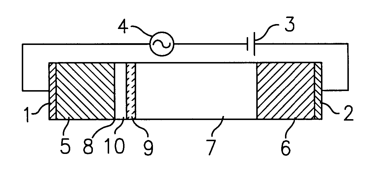
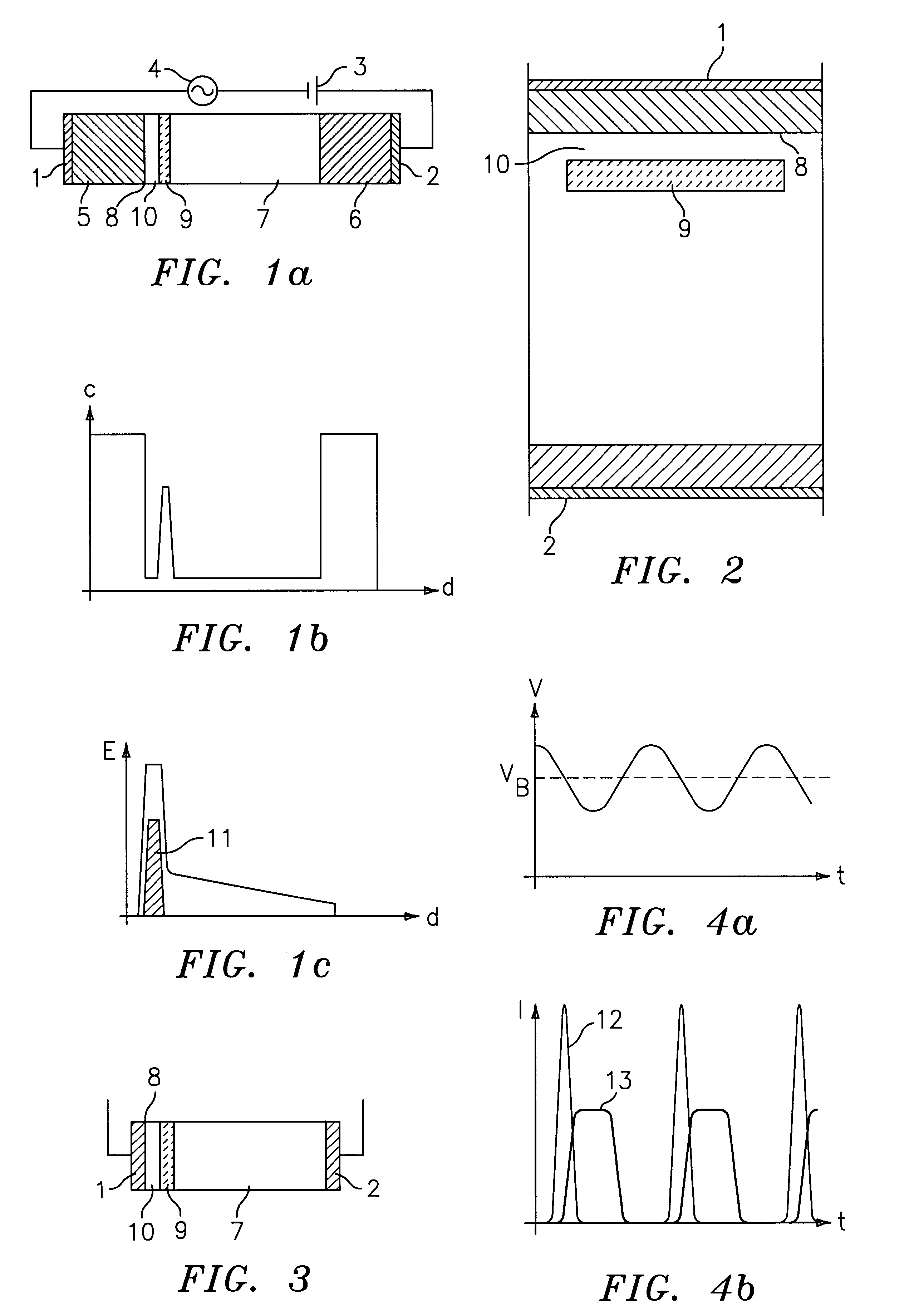
FIG. 1 illustrates a high power IMPATT (Impact Ionisation Avalanche Transit Time) diode for generation of power signals with a frequency above 30 GHz. This diode has two electrodes, namely a cathode 1 and an anode 2, adapted to be connected to a direct voltage source 3 and positioned in a microwave cavity 4 designed so as to have the resonance at desired microwave frequency. A semiconductor layer of crystalline SiC is arranged between the two electrodes and has a highly doped p-type layer 5 in contact with the metal cathode 1, a highly doped n-type layer 6 in contact with the metal anode 2, and a low doped n-type drift layer 7 interconnecting the layers 5 and 6. The layers 5 and 7 forms a pn-junction 8, which is reverse biased by the direct voltage of the direct voltage source 3. Furthermore, a thin n-type layer 9 with a substantially higher doping concentration than the drift layer is arranged in the drift layer 7 at a short distance from the highly doped p-type layer 5. The thin l...


PUM


Abstract

In a high power IMPATT ( Impact Avalanche Transit Time) diode for generating high frequency signals two electrodes, anode (2) and cathode (1), are arranged with a semiconductor layer therebetween. Said semiconductor layer comprises a drift layer (7) for transport of charge carriers between the electrodes. The semiconductor layer is made of crystalline SiC and it is provided with means (9) adapted to locally increase the electric field in the drift layer substantially with respect to the average electric field therein for generating an avalanche breakdown at a considerably lower voltage across the electrodes than would the electric field be substantially constant across the entire drift layer.

Description

FIELD OF THE INVENTION AND PRIOR ARTThe present invention relates to a high power IMPATT (Impact Avalanche Transit Time) diode for generating high frequency signals having two electrodes, an anode and a cathode, and a semiconductor layer therebetween with a junction for blocking conduction of the diode when a voltage is applied in a reverse direction across the electrodes, said semiconductor layer comprising a low doped n-type drift layer between the junction and a first of said electrodes through which charge carriers are transported upon avalanche breakdown in the semiconductor layer and avalanche multiplication of charge carriers when a voltage high enough is applied across the electrodes in said reverse direction.Such a diode employs the avalanche and carrier drift processes occurring in a semiconductor to produce a dynamic negative resistance at microwave frequencies. This diode is one of the most powerful sources of microwave power. It may be used to produce high power signals...

Claims


Application Information

Patent Timeline
IPC IPC(8): H01L29/66H01L29/864H01L29/02H01L29/24
CPCH01L29/864H01L29/1608
Inventor HARRIS, CHRISTOPHERKONSTANTINOV, ANDREI
Owner CREE SWEDEN
Why Eureka
Try Eureka