Isolation methods for leakage, loss and non-linearity mitigation in radio-frequency integrated circuits on high-resistivity silicon-on-insulator substrates

a radio-frequency integrated circuit and substrate technology, applied in the field of electronics, can solve the problems of reducing the overall resistivity of the bulk substrate, adversely affecting transistor performance, increasing the capacitive coupling in the soi substrate, etc., to reduce the non-linear effect of rf signals, reduce the coupling on rf transmission lines and losses, and reduce the cost

Inactive Publication Date: 2015-08-13
SKYWORKS SOLUTIONS INC
View PDF8 Cites 17 Cited by
  • Summary
  • Abstract
  • Description
  • Claims
  • Application Information

AI Technical Summary

Benefits of technology

This patented technology allows creating electronic components that are more efficient at transmitting data over long distances while also being less affected by external factors like electromagnetic interference or noise from other sources such as radio waves. It uses MOS structure instead of traditional methods called "passive," which helps reduce signal distortion caused by impedance mismatches between different parts inside an integrated circuit device's package.

Problems solved by technology

The technical problem addressed in this patents relating to improving resistance against current methods like ion implantations during production of advanced technology nodes (such as Fin FIGS), particularly when dealing with ultra-thin Si wafers due to their reduced size compared to traditional crystalline materials. Current techniques involve increasing conductance without adding extra layers, including dopants or impurities, leading to lower Q factors and unwanted side effect issues.

Method used


Image

  • Isolation methods for leakage, loss and non-linearity mitigation in radio-frequency integrated circuits on high-resistivity silicon-on-insulator substrates
  • Isolation methods for leakage, loss and non-linearity mitigation in radio-frequency integrated circuits on high-resistivity silicon-on-insulator substrates
  • Isolation methods for leakage, loss and non-linearity mitigation in radio-frequency integrated circuits on high-resistivity silicon-on-insulator substrates

Examples


Embodiment Construction

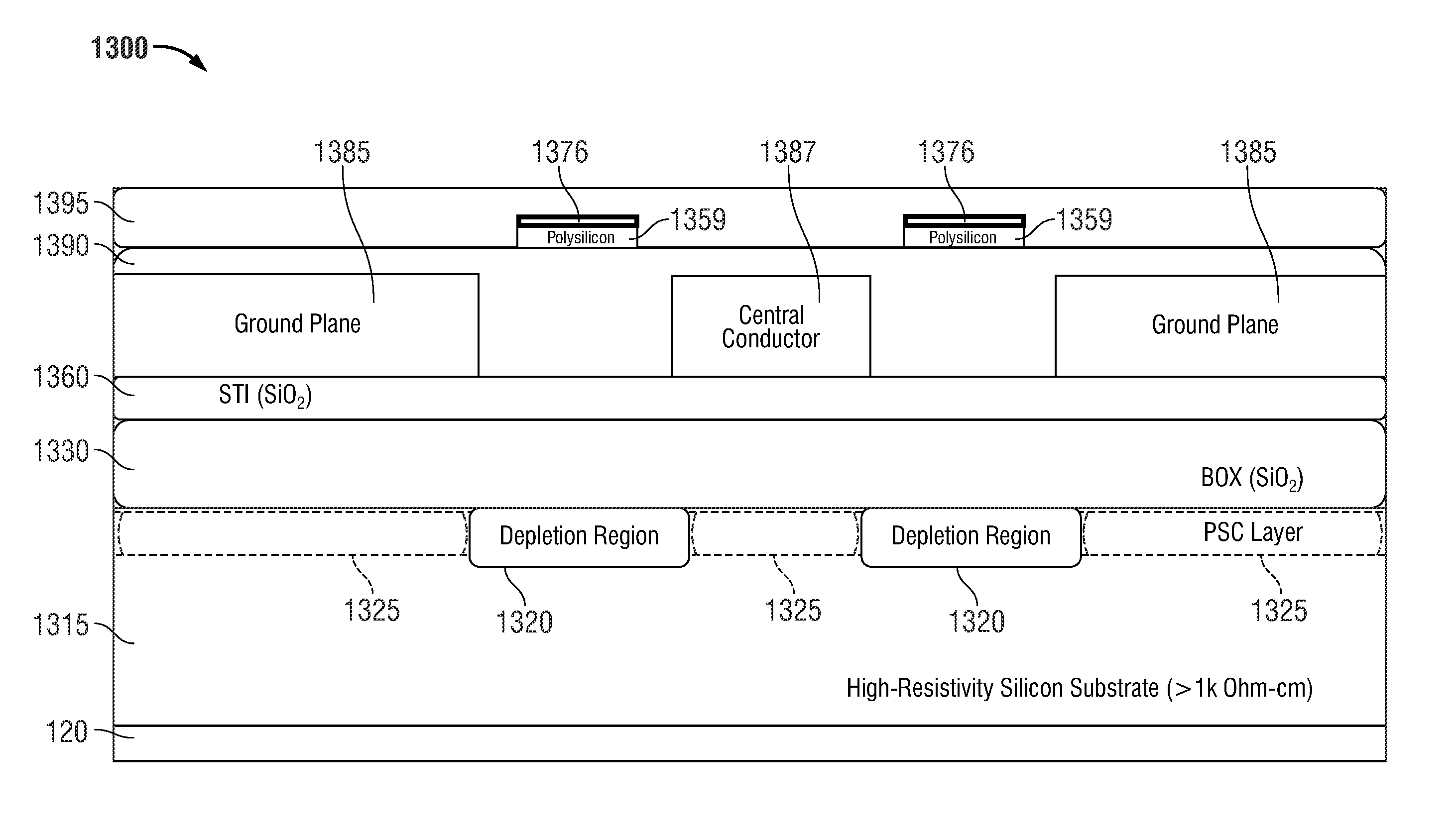
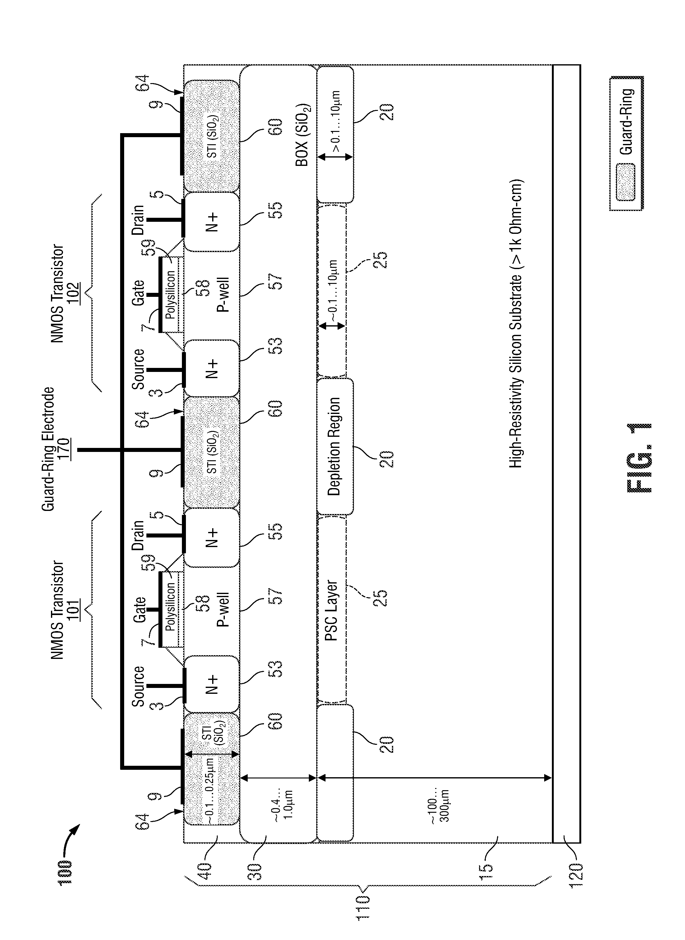
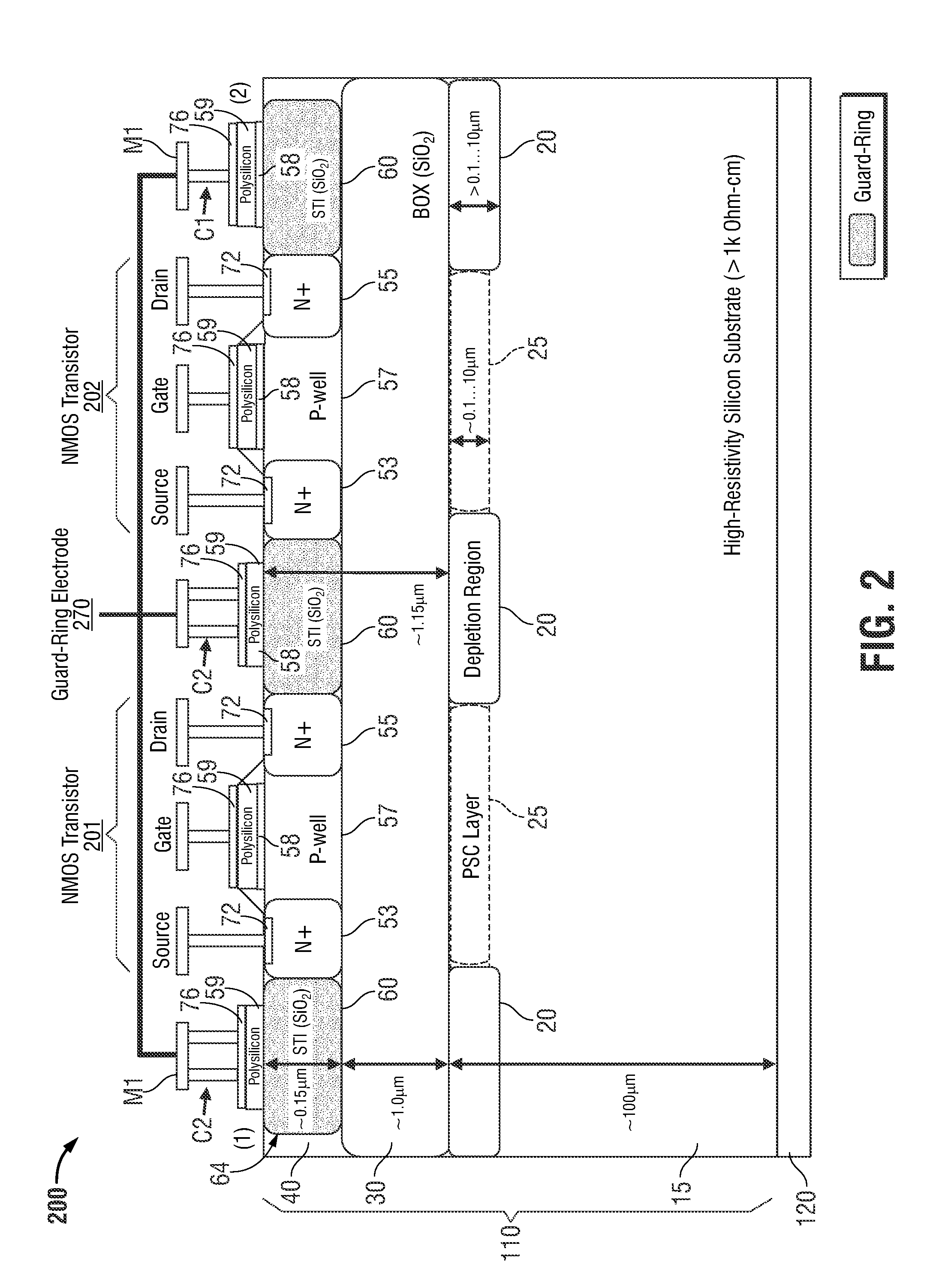
[0032]Hereinafter, embodiments of structures for implementing radio-frequency integrated circuits (RFICs) on high-resistivity silicon-on-insulator (SOI) substrates thereof, and methods of limiting a PSC layer in a RFIC, are described with reference to the accompanying drawings. Like reference numerals may refer to similar or identical elements throughout the description of the figures. It is understood that the following disclosure provides many different embodiments, or examples, for implementing different features of the invention. Specific examples of components and arrangements are described below to simplify the present disclosure. Many of the processes are known to one of skill in the art and are described in general detail only.

[0033]As it is used herein, the term ohms-cm (“ohms centimeter”) generally refers to the measurement of the volume resistivity (also known as bulk resistivity) of a semiconductor material. As used herein, “SOI transistors” generally refers to transistors


PUM


Abstract

A radio frequency integrated circuit with a silicon-on-insulator substrate includes a buried oxide layer that is disposed over a silicon substrate. The silicon-on-insulator substrate has a silicon layer that is disposed over the buried oxide layer. The integrated circuit includes a transistor disposed on the silicon layer, and a guard-ring in the silicon-on-insulator substrate that surrounds the transistor on the silicon layer. Depletion regions on the silicon substrate corresponding to areas surrounding the transistor is defined by the application of a voltage to the guard-ring. Isolation of radio frequency transmission lines on silicon-on-insulator substrates is also possible with this configuration.

Description


Claims


Application Information

Patent Timeline
Owner SKYWORKS SOLUTIONS INC
Why Eureka
Try Eureka