Electronic component
a technology of electronic components and components, applied in the direction of transformers/inductance details, inductances, coils, etc., can solve the problems of increasing the dimensions of the high-frequency coil b>500/b> in directions perpendicular to the layer stacking direction, and achieve the effect of downsizing an electronic componen
- Summary
- Abstract
- Description
- Claims
- Application Information
AI Technical Summary
Benefits of technology
Problems solved by technology
Method used
Image

Examples
first preferred embodiment
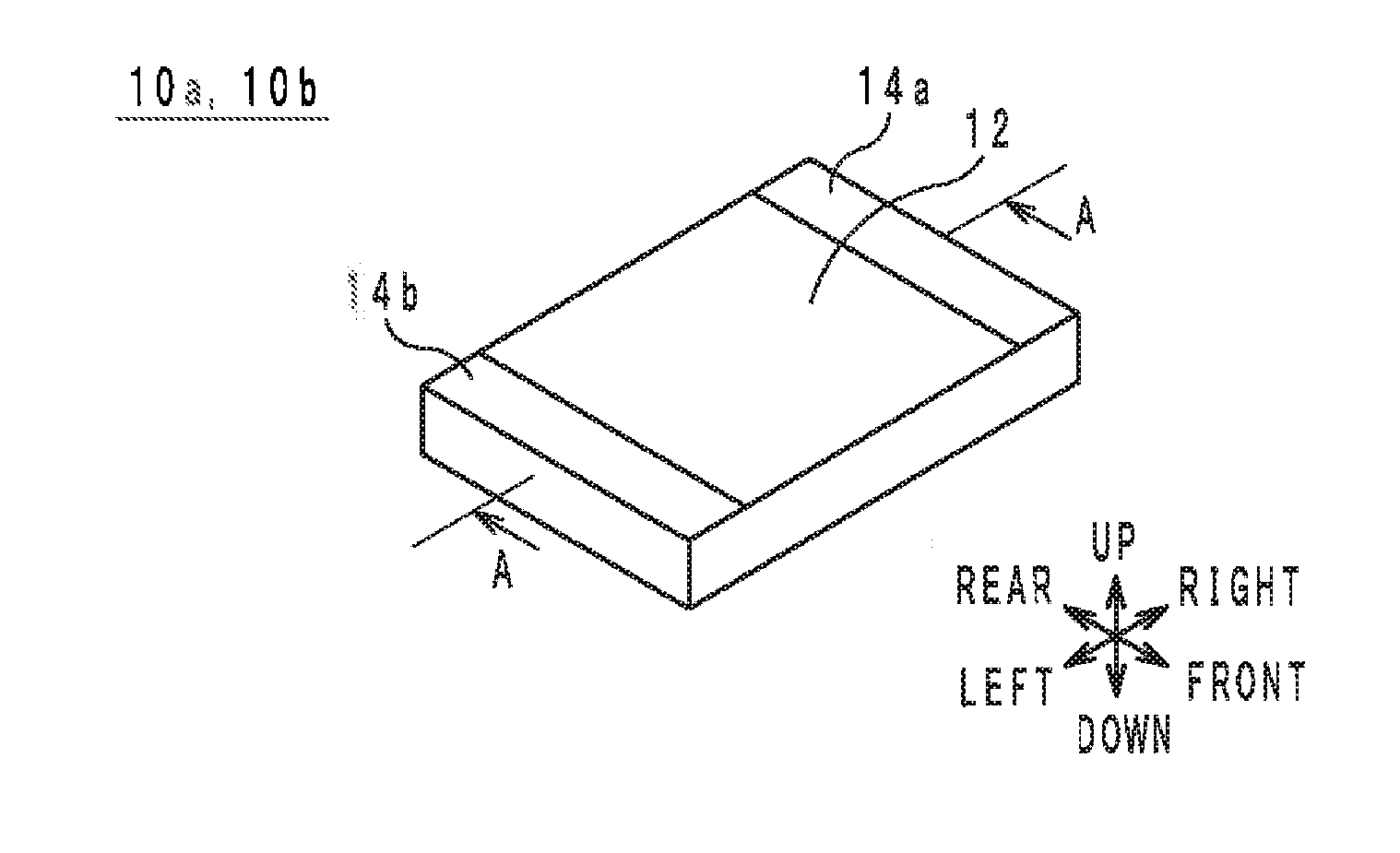
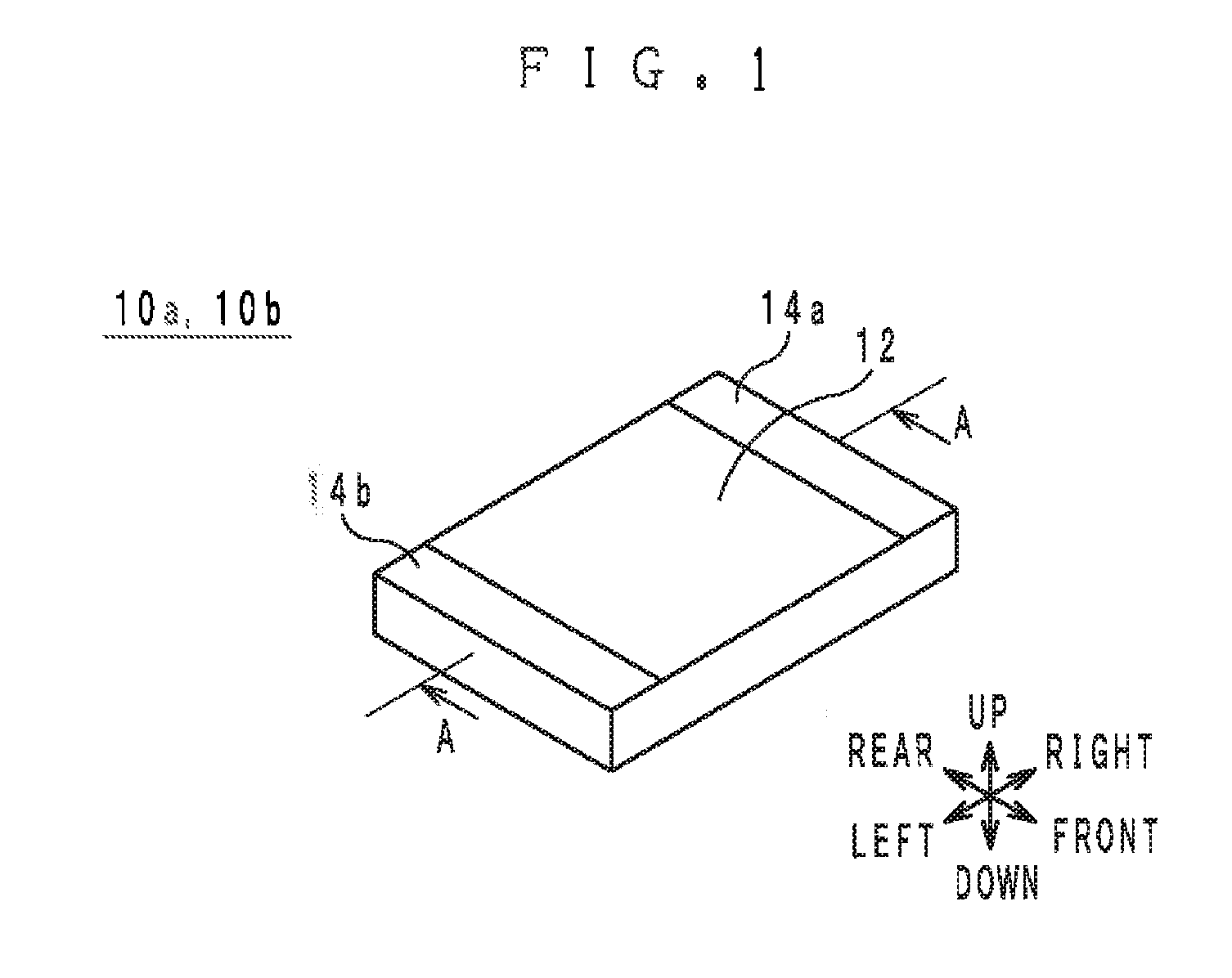
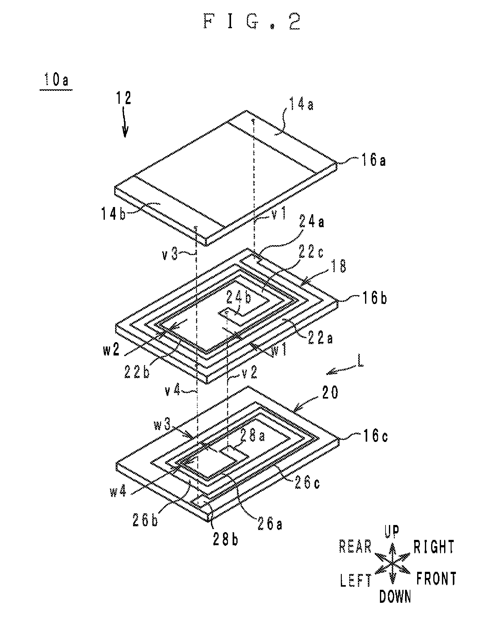
[0040]An electronic component according to a first preferred embodiment of the present invention will hereinafter be described with reference to the drawings. FIG. 1 is a perspective view of the electronic component 10a according to the first preferred embodiment. FIG. 2 is an exploded perspective view of the electronic component 10a according to the first preferred embodiment. FIG. 3A is a sectional view of the electronic component 10a cut along the line A-A. FIG. 3B is a plan view of coil conductors 18 and 20 of the electronic component 10a. In the following description, the layer stacking direction of the electronic component 10a is referred to as an up-down direction. In a top-down planar view, the direction in which longer sides of the electronic component 10a extend is referred to as a right-left direction, and the direction in which shorter sides of the electronic component 10a extend is referred to as a front-rear direction.
[0041]The electronic component 10a includes a multilay
second preferred embodiment
[0079]An electronic component according to a second preferred embodiment of the present invention will hereinafter be described with reference to the drawings. FIG. 8A is a perspective view of the electronic component 10b according to the second preferred embodiment. FIG. 8B is a plan view of coil conductors 20 and 19 of the electronic component 10b. FIG. 8C is a plan view of the coil conductor 19 and a coil conductor of the electronic component 10b. The appearance of the electronic component 10b is as illustrated in FIG. 1.
[0080]The electronic component 10b differs from the electronic component 10a in that the coil conductors 19 and 21 are further provided. More specifically, the multilayer body 12 of the electronic component 10b includes dielectric layers 16a-16e stacked in this order from the top to the bottom. The coil L of the electronic component 10b includes the coil conductors 18, 20, 19 and 21 connected in series in this order.
[0081]The coil conductors 18 and 20 are provided o
third preferred embodiment
[0096]An electronic component according to a third preferred embodiment of the present invention will hereinafter be described with reference to the accompanying drawings. FIG. 9 is a perspective view of the electronic component 10c according to the third preferred embodiment. FIG. 10A is an exploded perspective view of the electronic component 10c according to the third preferred embodiment. FIG. 10B is a plan view of coil conductors 50 and 52 of the electronic component 10c.
[0097]The electronic component 10c includes a multilayer body 12, external electrodes 14a-14d, and coils L1 and L2. As seen in FIGS. 9 and 10A, the multilayer body 12 is a rectangular or substantially rectangular plate in a top-down planar view. The multilayer body 12 includes dielectric (insulating) layers 16a-16e stacked in this order from the top to the bottom. The dielectric layers 16a-16e are rectangular or substantially rectangular and are made of a flexible dielectric material, for example, liquid crystal
PUM
 Abstract
Description
Claims
Application Information
 - R&D Engineer
- R&D Manager
- IP Professional
- Industry Leading Data Capabilities
- Powerful AI technology
- Patent DNA Extraction
Browse by: Latest US Patents, China's latest patents, Technical Efficacy Thesaurus, Application Domain, Technology Topic.
© 2024 PatSnap. All rights reserved.Legal|Privacy policy|Modern Slavery Act Transparency Statement|Sitemap