Advanced node cost reduction by ESD interposer

Active Publication Date: 2018-07-19
INTEL CORP
View PDF4 Cites 8 Cited by
  • Summary
  • Abstract
  • Description
  • Claims
  • Application Information

AI Technical Summary

Problems solved by technology

ESD structures are generally relatively area consuming and their size generally cannot be reduced in the manner that typical digital circuits have

Method used


Image

  • Advanced node cost reduction by ESD interposer
  • Advanced node cost reduction by ESD interposer
  • Advanced node cost reduction by ESD interposer

Examples


examples

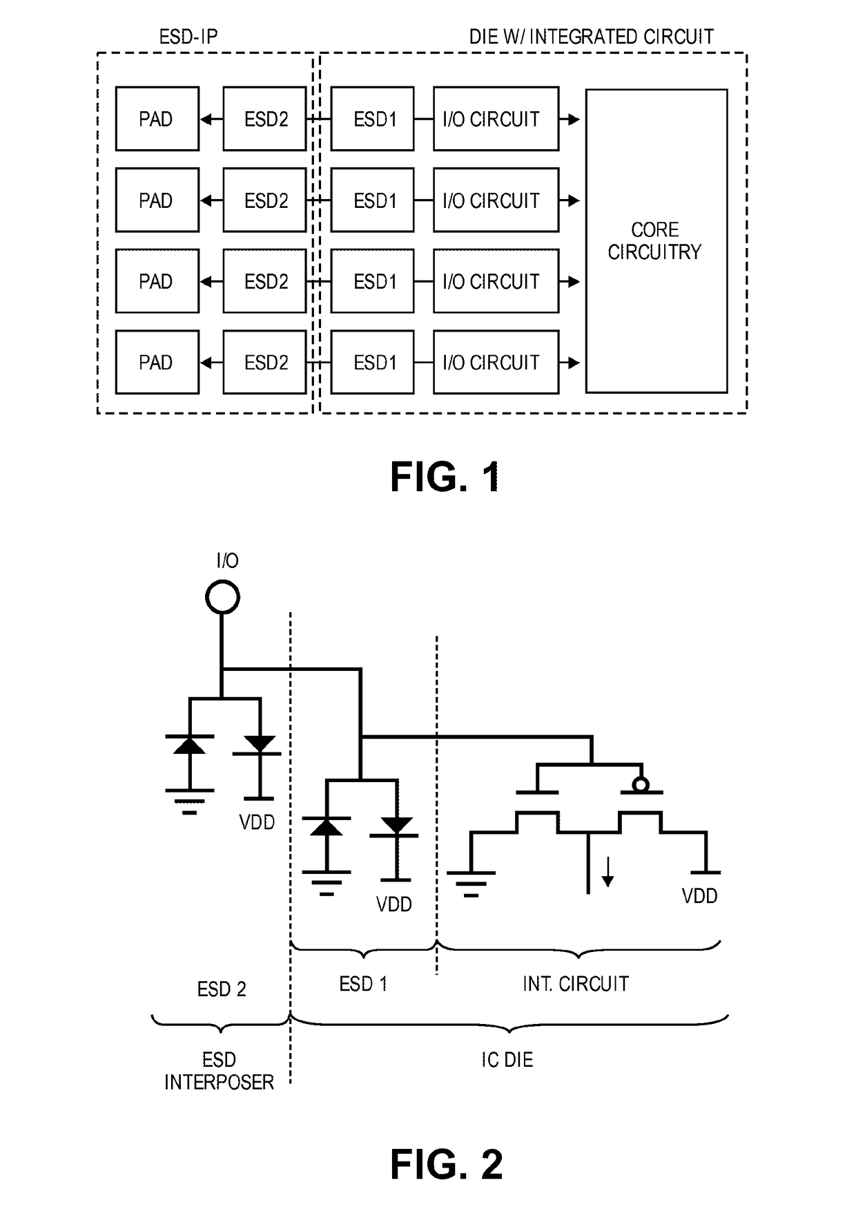
[0076]Example 1 is an apparatus including an electrostatic discharge circuit including a first circuit portion coupled beneath a die contact pad of an integrated circuit die and a second circuit portion in an interposer separate from the integrated circuit die, the interposer including a first contact point coupled to the contact pad of the integrated circuit die and a second contact point operable for connection to an external source.

[0077]In Example 2, the first circuit portion in the apparatus of Example 1 includes an ESD robustness that is different than an ESD protection robustness of the second circuit portion.

[0078]In Example 3, the first circuit portion in the apparatus of Example 2 includes a smaller maximum discharge current than a maximum discharge current of the second circuit portion and a failure threshold and failure threshold voltage of the second circuit portion is less than a failure threshold voltage of the first circuit portion.

[0079]In Example 4, the interposer in


PUM


Abstract

An apparatus including an electrostatic discharge circuit including a first circuit portion coupled beneath a die contact pad of an integrated circuit die and a second circuit portion in an interposer separate from the integrated circuit die, the interposer including a first contact point coupled to the contact pad of the integrated circuit die and a second contact point operable for connection to an external source. A method including forming an integrated circuit die including a first electrostatic discharge structure beneath a contact pad of the die; and coupling the die to an interposer including an interposer contact and a second electrostatic discharge structure, wherein a signal at the contact pad of the die is operable to be routed through the interposer.

Description


Claims


Application Information

Patent Timeline
Owner INTEL CORP
Why Eureka
Try Eureka