Method of and Apparatus for Forming Three-Dimensional Structures Integral With Semiconductor Based Circuitry

Inactive Publication Date: 2007-08-30
COHEN ADAM L +1
View PDF28 Cites 2 Cited by
  • Summary
  • Abstract
  • Description
  • Claims
  • Application Information

AI Technical Summary

Benefits of technology

[0053] It is an object of some embodiments of various aspects of the present invention to provide simpler processes for integrating electrochemically fabricated multilayer structures with integrated circuits.
[0054] It is an object of

Problems solved by technology

The CC mask plating process is distinct from a “through-mask” plating process in that in a through-mas

Method used


Image

  • Method of and Apparatus for Forming Three-Dimensional Structures Integral With Semiconductor Based Circuitry
  • Method of and Apparatus for Forming Three-Dimensional Structures Integral With Semiconductor Based Circuitry
  • Method of and Apparatus for Forming Three-Dimensional Structures Integral With Semiconductor Based Circuitry

Examples


Embodiment Construction

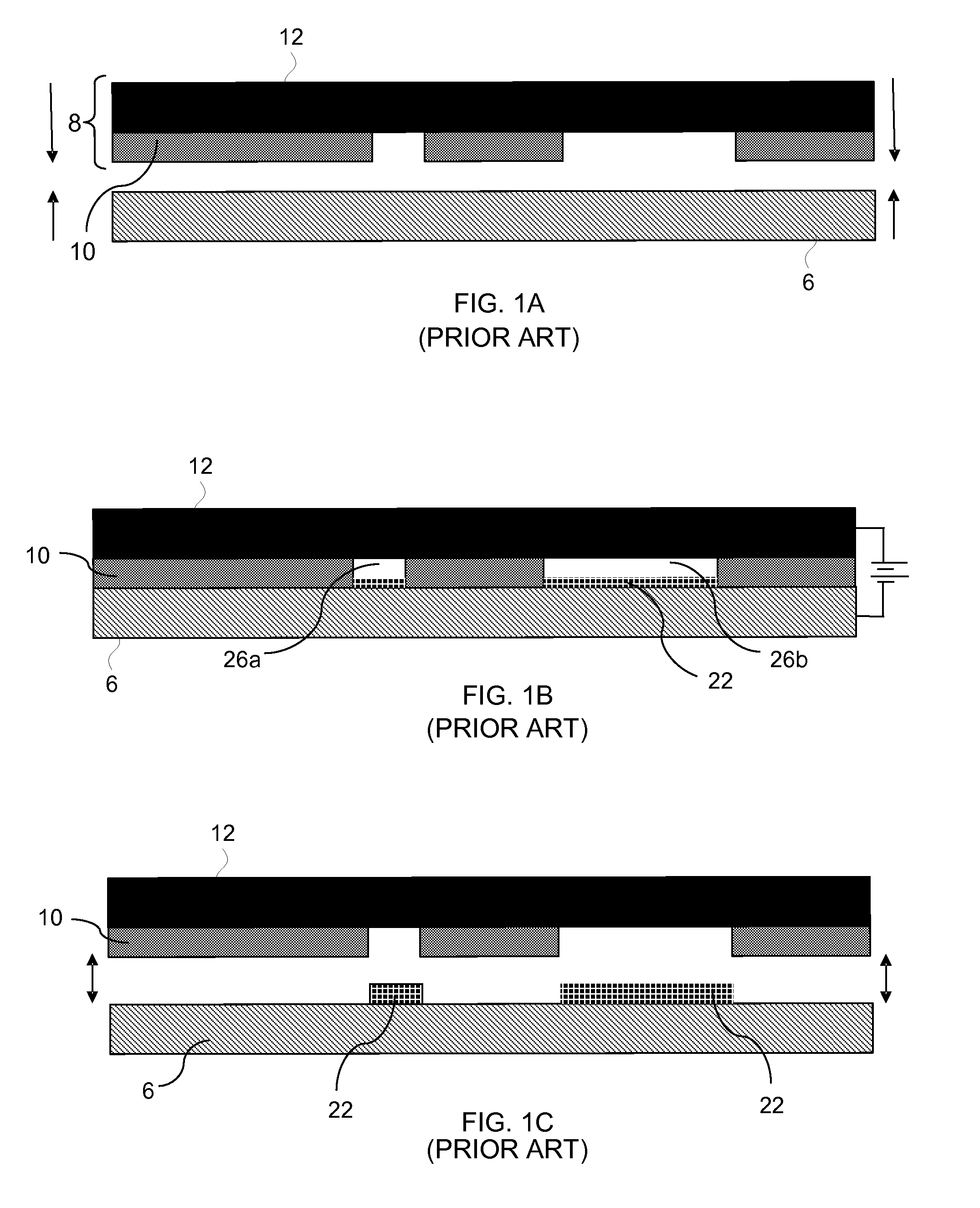
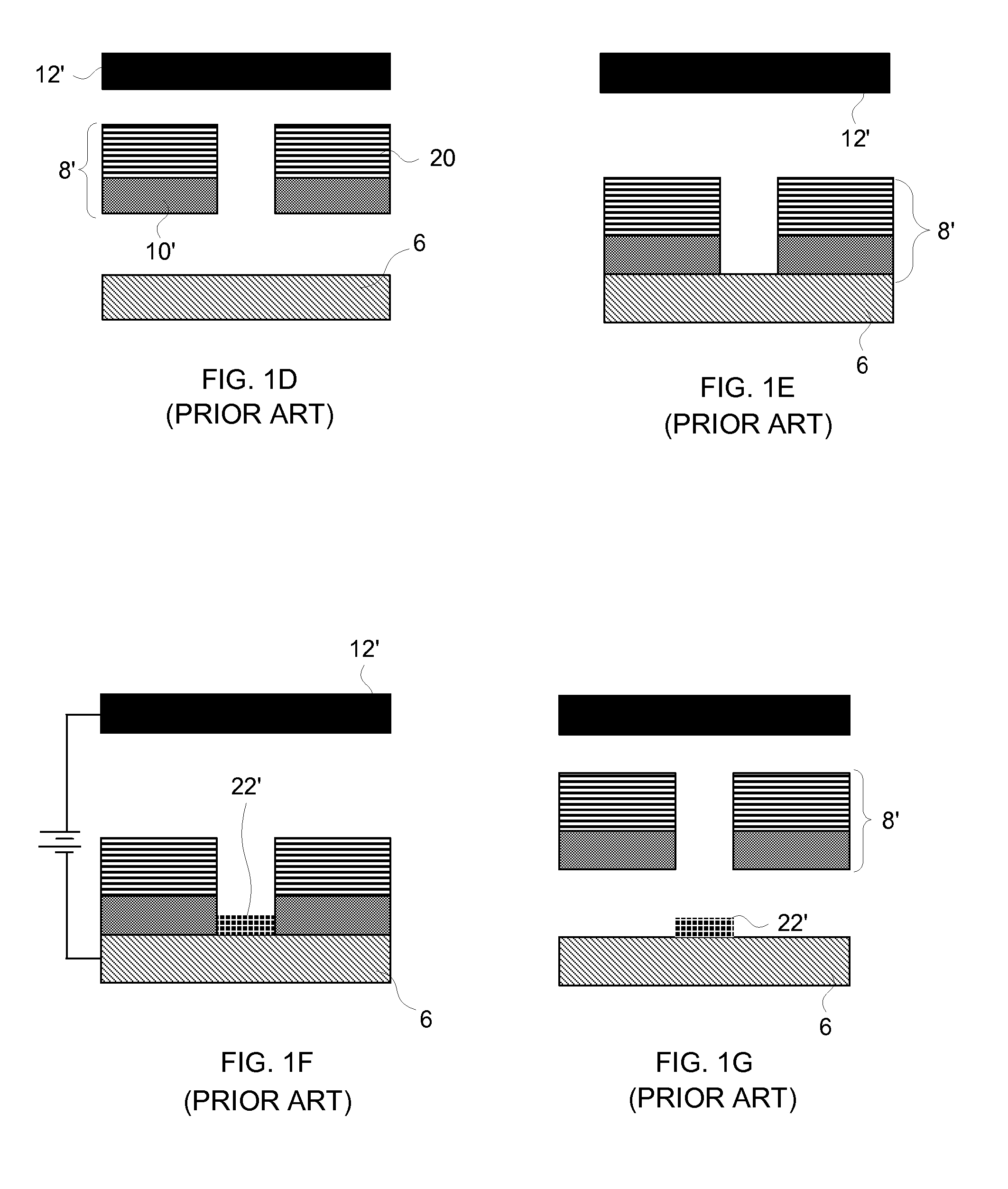
[0074]FIGS. 1A-1G, 2A-2F, and 3A-3C illustrate various features of one form of electrochemical fabrication that are known. Other electrochemical fabrication techniques are set forth in the '630 patent referenced above, in the various previously incorporated publications, in various other patents and patent applications incorporated herein by reference, still others may be derived from combinations of various approaches described in these publications, patents, and applications, or are otherwise known or ascertainable by those of skill in the art from the teachings set forth herein. All of these techniques may be combined with those of the various embodiments of various aspects of the invention to yield enhanced embodiments. Still other embodiments may be derived from combinations of the various embodiments explicitly set forth herein.

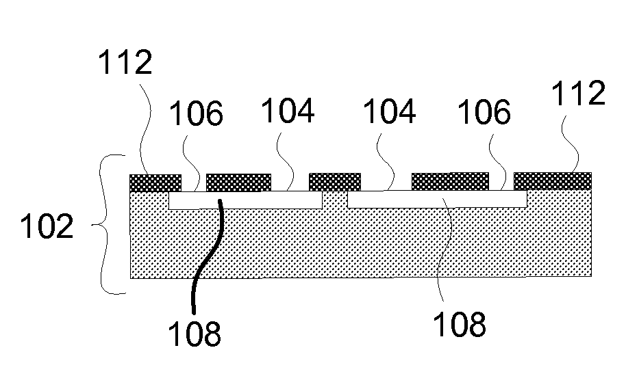
[0075]FIGS. 4A-4F illustrate various stages in the formation of a single layer of a multi-layer fabrication process where a second metal is deposited on


PUM

PropertyMeasurementUnit
Thicknessaaaaaaaaaa
Diffusion barrieraaaaaaaaaa
Adhesion strengthaaaaaaaaaa

Abstract

Enhanced Electrochemical fabrication processes are provided that can form three-dimensional multi-layer structures using semiconductor based circuitry as a substrate. Electrically functional portions of the structure are formed from structural material (e.g. nickel) that adheres to contact pads of the circuit. Aluminum contact pads and silicon structures are protected from copper diffusion damage by application of appropriate barrier layers. In some embodiments, nickel is applied to the aluminum contact pads via solder bump formation techniques using electroless nickel plating. In other embodiments, selective electroless copper plating or direct metallization is used to plate sacrificial material directly onto dielectric passivation layers. In still other embodiments, structural material deposition locations are shielded, then sacrificial material is deposited, the shielding is removed, and then structural material is deposited. In still other embodiments structural material is made to attach to non-contact pad regions.

Description


Claims


Application Information

Patent Timeline
Owner COHEN ADAM L
Why Eureka
Try Eureka