Process for producing wiring substrate
a technology of wiring substrate and substrate, which is applied in the direction of dielectric characteristics, thermoplastic polymer dielectrics, printed element electric connection formation, etc., can solve the problems of low surface energy of fluororesin such as ptfe, insufficient bonding of plating layers, and failure to meet electrical properties, etc., to achieve excellent electrical properties
- Summary
- Abstract
- Description
- Claims
- Application Information
AI Technical Summary
Benefits of technology
Problems solved by technology
Method used
Image

Examples
first embodiment
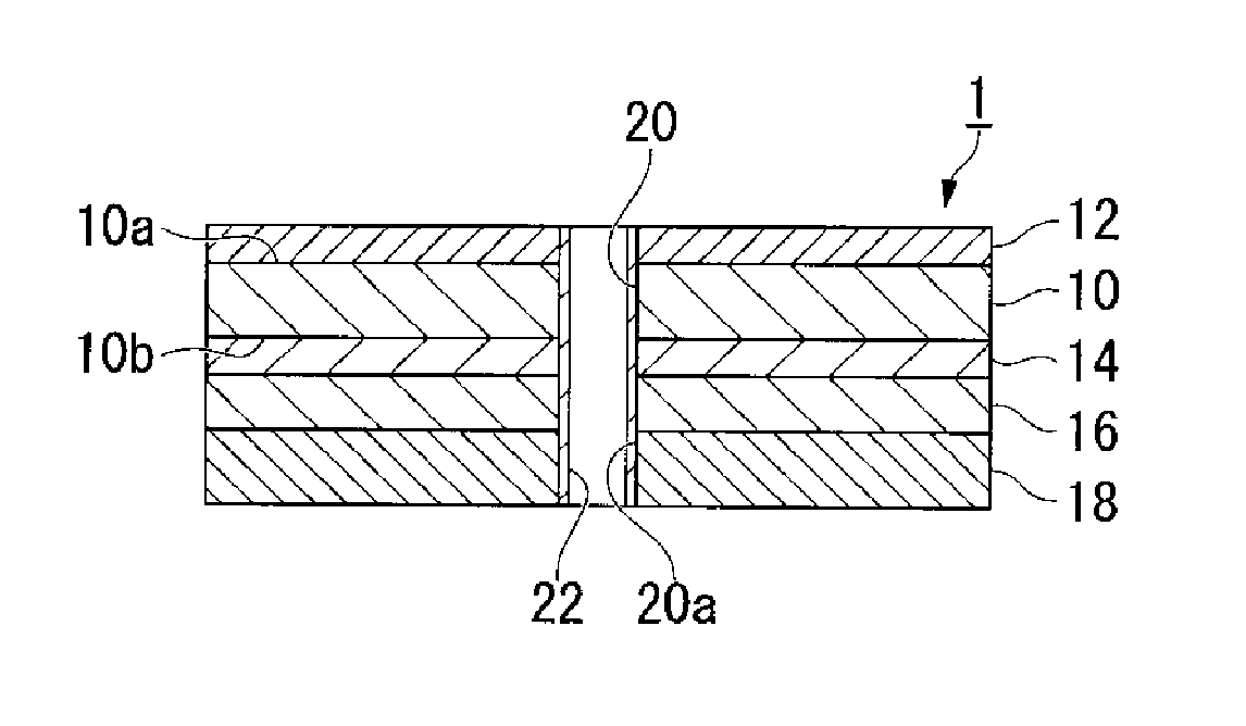
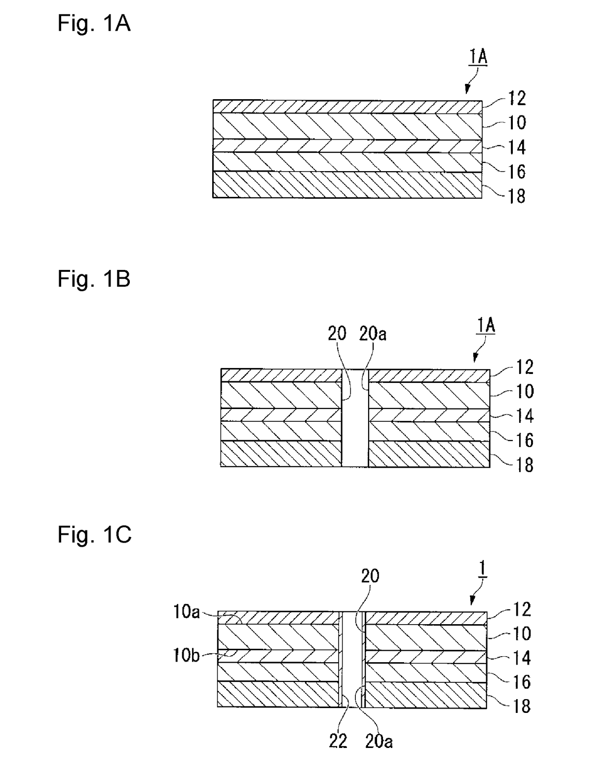
[0180]In a case where the wiring substrate 1 is produced by the process (i), a laminate 1A having a layer structure of first conductor layer 12 / layer (A) 10 / second conductor layer 14 / adhesive layer 16 / layer (B) 18 as shown in FIG. 1A is used. As shown in FIG. 1B, a hole 20 which penetrates from the first conductor layer 12 through the layer (B) 18 is formed in the laminate 1A e.g. by a drill or laser. Then, either one or both of a treatment with a permanganic acid solution and a plasma treatment is applied to an inner wall surface 20a of the hole 20 formed without conducting an etching treatment using metal sodium, and then as shown in FIG. 1C, e.g. electroless plating is applied to the inner wall surface 20a of the hole 20 to form a plating layer 22.
second embodiment
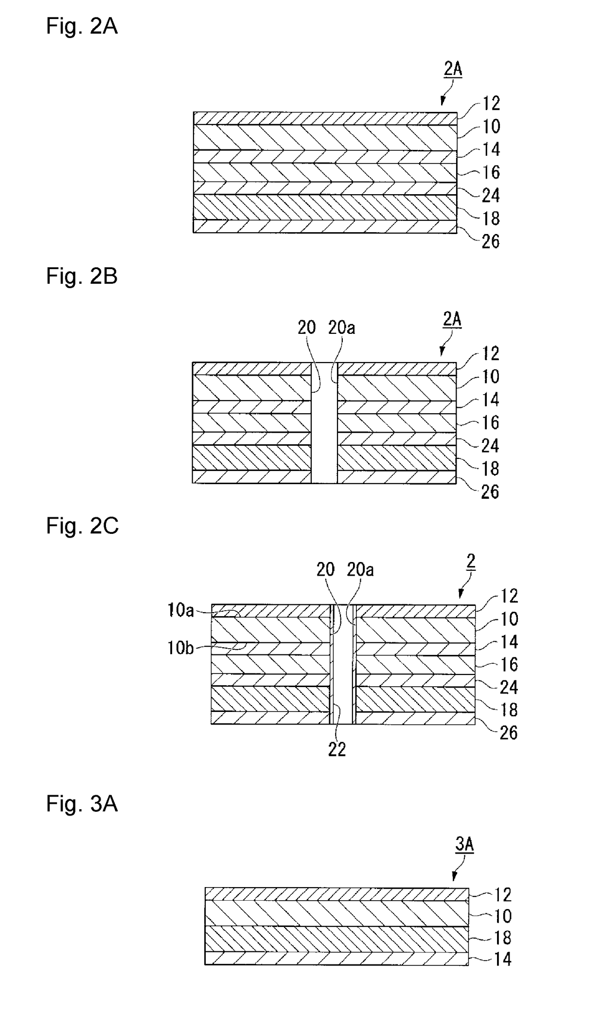
[0181]In a case where a wiring substrate 2 is produced by the process (i), a laminate 2A having a layer structure of first conductor layer 12 / layer (A) 10 / second conductor layer 14 / adhesive layer 16 / third conductor layer 24 / layer (B) 18 / fourth conductor layer 26, as shown in FIG. 2A, is used. In the same manner as in the case of the wiring substrate 1, as shown in FIG. 2B, a hole 20 which penetrates from the first conductor layer 12 through the fourth conductor layer 26 is formed in the laminate 2A. Then, either one or both of a treatment with a permanganic acid solution and a plasma treatment is applied to an inner wall surface 20a of the hole 20 formed without conducting an etching treatment using metal sodium, and then as shown in FIG. 2C, a plating layer 22 is formed on the inner wall surface 20a of the hole 20.
third embodiment
[0182]In a case where a wiring substrate 3 is produced by the process (i), a laminate 3A having a layer structure of first conductor layer 12 / layer (A) 10 / layer (B) 18 / second conductor layer 14, as shown in FIG. 3A, is used. In the same manner as in the case of the wiring substrate 1, as shown in FIG. 3B, a hole 20 which penetrates from the first conductor layer 12 through the second conductor layer 14 is formed in the laminate 2A. Then, either one or both of a treatment with a permanganic acid solution and a plasma treatment is applied to an inner wall surface 20a of the hole 20 formed without conducting an etching treatment using metal sodium, and then as shown in FIG. 3C, a plating layer 22 is formed on the inner wall surface of the hole 20.
PUM
| Property | Measurement | Unit |
|---|---|---|
| Temperature coefficient of resistance | aaaaa | aaaaa |
| Content | aaaaa | aaaaa |
| Dielectric constant | aaaaa | aaaaa |
Abstract
Description
Claims
Application Information
 - R&D Engineer
- R&D Manager
- IP Professional
- Industry Leading Data Capabilities
- Powerful AI technology
- Patent DNA Extraction
Browse by: Latest US Patents, China's latest patents, Technical Efficacy Thesaurus, Application Domain, Technology Topic.
© 2024 PatSnap. All rights reserved.Legal|Privacy policy|Modern Slavery Act Transparency Statement|Sitemap