Ion-Doped Two-Dimensional Nanomaterials
- Summary
- Abstract
- Description
- Claims
- Application Information
AI Technical Summary
Benefits of technology
Problems solved by technology
Method used
Image

Examples
example 1
Ion-Based Gating of Graphene.
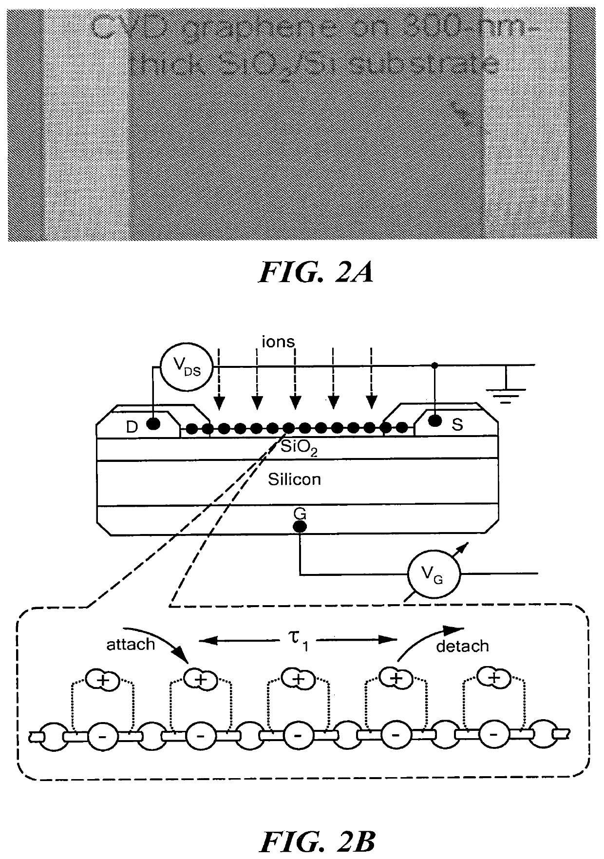
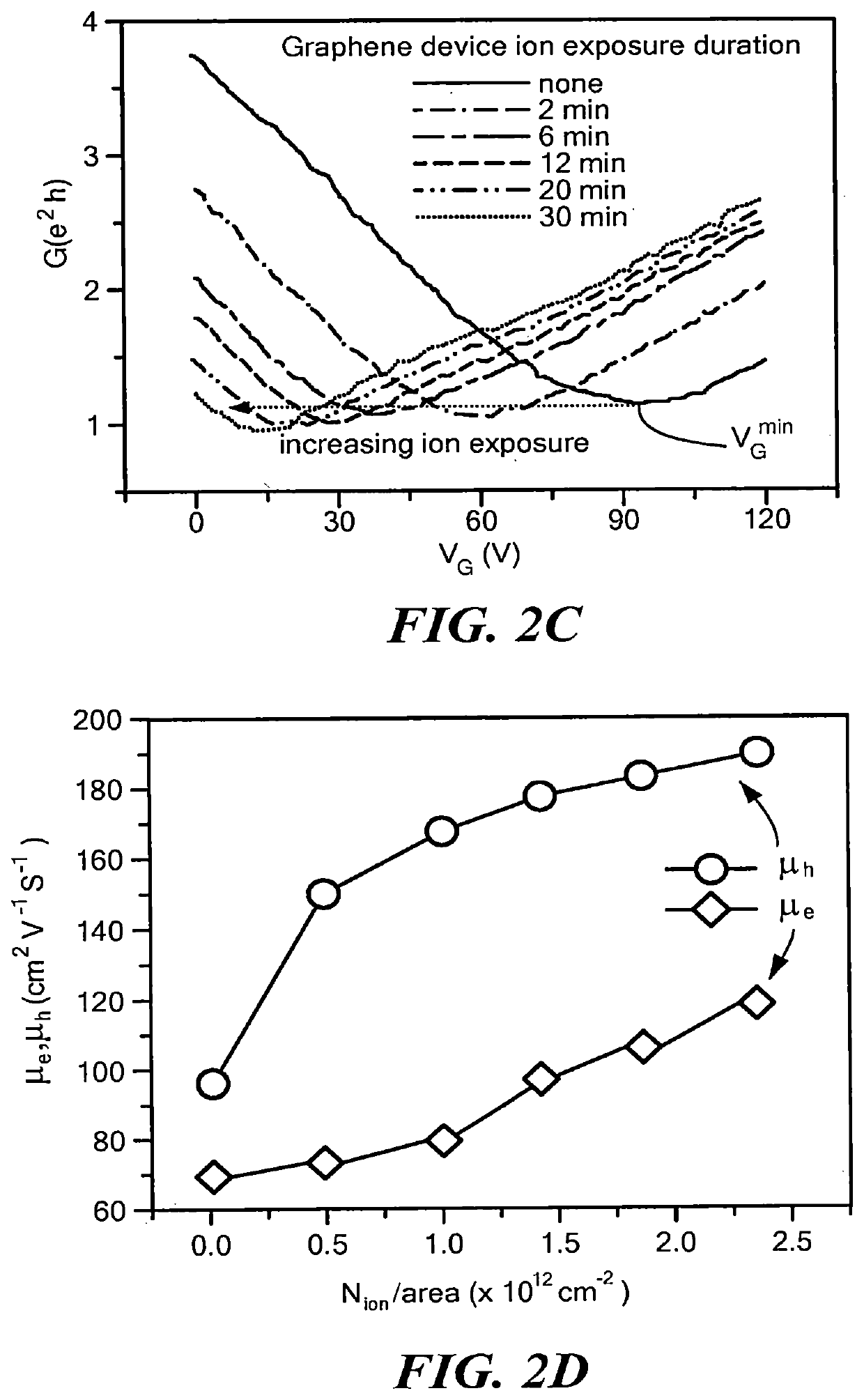
[0062]Ion-exposure experiments were performed on a variety of nanomaterials, both under vacuum (P˜10−5 Torr, using Granville Phillips Ionization Gauge Model No. 274003, producing primarily N2+) as well as in open air (Ion Projector Model No. NIP-6E), the generated ion flux was directed from the ionization gauge towards the device); both conditions were found to be equally effective. FIGS. 2A-2D outline the results of ion-incidence experiments on a gated, 3-terminal graphene device (shown in FIGS. 2A, 2B), in which the metal-graphene contact area was covered with a photoresist layer to eliminate any contact-induced effect. If the incident positive ions were to absorb electrons from graphene, they would induce holes (i.e. p-type doping) that should right-shift the transconductance curves towards higher positive values. In contrast (FIG. 2C), starting with an intrinsically p-doped device, the exposure to incident positive ions led to the curves being left-shif
example 2
Ion-Based Gating of Molybdenum Disulfide in an FET Device.
[0063]FIGS. 3A-3E summarize an experiment similar to Example 1 but performed on a monolayer MoS2 FET device. A monolayer of atomically thin MoS2 was made by chemical vapor deposition, resulting in an optoelectronic grade crystalline quality film. WO2016 / 133570 describes methods of making ultrathin MoS2 films. As in the previous case, the contact areas were protected with photoresist prior to ion-exposure. In this study, the devices were tested with both positive and negative ions. Different devices were used to eliminate any “history” effect. FIGS. 3C and 3D show how the transfer characteristics shifted to the left (indicating n-type doping in case of positive ions) and to the right (indicating p-type doping in case of negative ions). The transfer curves recovered (as seen in FIG. 3D) after overnight release, indicating that the ions did not form any chemical bonds. The induced carrier density was estimated using the formula Δ
example 3
Stabilization of Ion-Doping by Addition of a Capping Layer.
[0064]Carrier-induction as demonstrated in Examples 1 and 2 remained effective as long as the ion source remained on, and stable doping levels could be achieved by controlling the source rate once the desired doping level had been achieved. However, while this approach was quite effective for investigating a variety of fundamental questions, for practical applications the doping effect must be stabilized.
[0065]Devices were capped with a freshly cured insulating polydimethylsiloxane (PDMS) thin film. FIGS. 4A-4E summarize the experimental results obtained where the release and recovery of the channel current in a set of devices using a single-wall carbon nanotube (SWNT) film; the devices were of similar geometry and resistance. The devices (shown in FIGS. 4A, 4B) were studied under various pressure and capping conditions over several days. In all devices, the channel current was monitored under a fixed bias (0.2V) after 2 mins o
PUM
| Property | Measurement | Unit |
|---|---|---|
| Thickness | aaaaa | aaaaa |
| Thickness | aaaaa | aaaaa |
| Electric potential / voltage | aaaaa | aaaaa |
Abstract
Description
Claims
Application Information
 - R&D Engineer
- R&D Manager
- IP Professional
- Industry Leading Data Capabilities
- Powerful AI technology
- Patent DNA Extraction
Browse by: Latest US Patents, China's latest patents, Technical Efficacy Thesaurus, Application Domain, Technology Topic.
© 2024 PatSnap. All rights reserved.Legal|Privacy policy|Modern Slavery Act Transparency Statement|Sitemap