Formation method of semiconductor structure

A semiconductor and graphics technology, which is applied in semiconductor devices, semiconductor/solid-state device manufacturing, electric solid-state devices, etc., can solve the problems of increasing the difficulty and complexity of integrated circuits, achieve good graphics effects, improve matching, and improve graphics accuracy Effect

Pending Publication Date: 2022-05-27
SEMICON MFG INT (SHANGHAI) CORP +1
View PDF0 Cites 0 Cited by
  • Summary
  • Abstract
  • Description
  • Claims
  • Application Information

AI Technical Summary

Benefits of technology

This patented technology allows for easier formation of structures with specific properties through selective addition or removal of certain materials during fabrication processes without affecting other layers. By doing this, these structures have more precise dimensions and match their designed requirements compared to traditional methods like lithography.

Problems solved by technology

The technical problem addressed during this patented research relates to improving the accuracy or consistency with which patterns are transferred onto wafers for integration into electronic devices such as computers. This requires reducing the sizes of these patterns while maintaining their precise dimensions, resulting in difficulties when trying to match them accurately.

Method used


Image

  • Formation method of semiconductor structure
  • Formation method of semiconductor structure
  • Formation method of semiconductor structure

Examples


Embodiment Construction

[0023] It can be seen from the background art that how to improve the matching degree between the target pattern and the design pattern formed on the wafer has become a challenge.

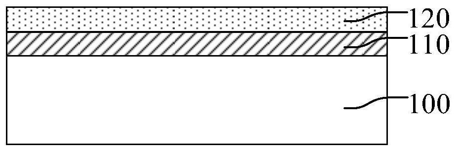
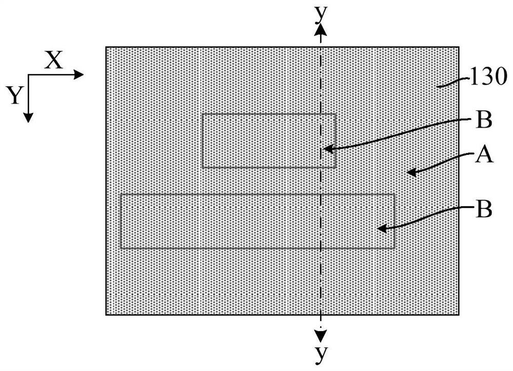
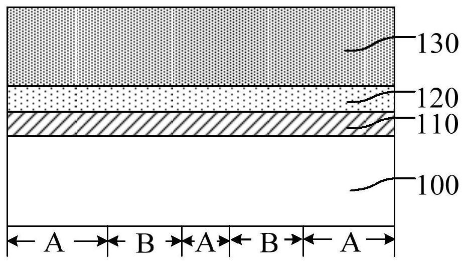
[0024] In order to solve the technical problem, an embodiment of the present invention provides a method for forming a semiconductor structure, including: providing a substrate, including a target layer for forming a target pattern; forming a core layer on the substrate, and the core layer includes The anti-etch area for forming the anti-etch layer and the sacrificial area for forming the sacrificial layer; ion doping is carried out to the core layer of the sacrificial area, which is suitable for making the core layer of the sacrificial area and the anti-etch area The etched rate of the core layer is different, the core layer doped with ions in the sacrificial region is used as a sacrificial layer, and the core layer not doped with ions in the anti-etching region is used as an anti-etching layer; Form


PUM


Abstract

The invention discloses a forming method of a semiconductor structure. The forming method comprises the steps of providing a substrate; forming a core layer on the substrate; ion doping is carried out on the core layer of the sacrificial region, so that the etching rates of the core layer of the sacrificial region and the core layer of the anti-etching region are different, the core layer doped with ions is used as a sacrificial layer, and the core layer not doped with ions is used as an anti-etching layer; forming a groove penetrating through the core layer between the adjacent sacrificial regions; side walls are formed on the side walls of the groove, and the side walls located on the side walls of the groove define a first groove; the sacrificial layer is removed through an etching process, a second groove penetrating through the anti-etching layer is formed, and the etching rate of the etching process on the sacrificial layer is larger than that of the anti-etching layer; and etching the target layer at the bottoms of the first groove and the second groove by taking the anti-etching layer and the side wall as masks to form a target pattern. According to the embodiment of the invention, the pattern precision of the target pattern and the matching degree of the target pattern and the design pattern can be improved.

Description


Claims


Application Information

Patent Timeline
Owner SEMICON MFG INT (SHANGHAI) CORP
Why Eureka
Try Eureka